4 Layer PCB Layout Using EasyEDA Step By Step Tutorial
Online PCB Design and Manufacturing
In the previous post, I showed you how you can use EasyEDA and JLCPCB to design 2 layer PCB Online, create PCB layout and order them online. That was fun and easy right?
In this post, we will be taking a look at how to design 4 Layer PCB and create PCB Layout using EasyEDA and JLCPCB.


EasyEDA and JLCPCB
In simple words, EasyEDA is an easier but powerful online PCB design tool which allows electronics engineers, hackers, educators, hobbyists, makers, and enthusiasts to design and share their projects’ schematics as well as PCB layout. This is a design tool integrated LCSC components catalog and JLCPCB PCB service that helps users to save time to make their ideas into real products.
At EasyEDA, you will see Thousands of Open Source as well as Private Projects at your disposal. You can also make your own public projects including various components and circuit simulations. You can tap into this huge collection of Robotics/Home Automation/Hobby projects schematics and layout and speed up your design.
What is a 2 Layer PCB?
Depending up on the complexity, the PCB can be 2 layer or extend up to 8 layers. As you know, PCBs are basically a bunch of tiny copper wires sandwiched in between multiple layers of fiberglass. These tiny wires connect all the components to each other in an organized and repeatable way making a neat and tidy electronic circuit board. Adding each layer means adding 2 more layers . Simples of multilayer PCB is the 2-layer PCB.

For a 2 layer PCB, there is a Top Layer and a Bottom Layer. 2 Layer PCB can accommodate and connect components to each other using copper tracks on both sides of the board. Routing on both sides can be connected using sepecial holes made using conductive materials which are made across the board. Now take a look at the 4 Layer PCB
Why do we use 4 Layer PCB?
In the case of a 4 Layer PCB, there are actually 4 layers of conductive copper material. There is a Top layer – the one on the top, a Bottom Layer – One on the bottom and 2 more layers sandwiched in between Top and Bottom Layer; we call it inner layer 1 and inner layer 2.
Here, routing can be made on all the four layers which helps us to do more routing in low surface area. This means you have to draw layout on all the layers/surfaces at the same time connecting them at certain points.
Luckily, we have online PCB designing tools from Easy EDA, provides all the necessary capability for online PCB Design and PCB Printing of Circuit Boards with hundreds of components and multiple layers with thousands of tracks.
4 Layer PCB Video Tutorial

Advantages of 4 Layer PCB
- Increase Functionality of the board without an increase in area
- Reduce PCB Size
- Reduce in PCB Size leads to the Reduce in PCB weight
- Increases Density of Assembly
- Light Weight
- Enhanced Flexibility
4 Layer PCB Layout Tutorial
Follow these steps to get started with 4 Layer PCB Layout and Designing.
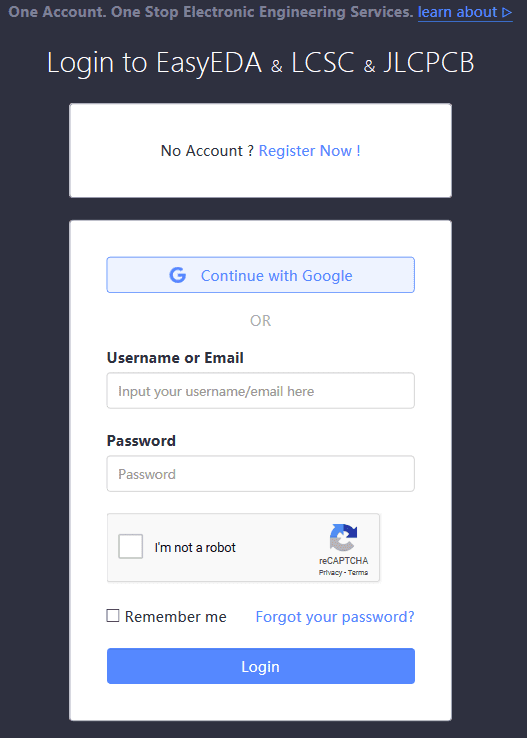
Step 1 : Create an Account in EasyEDA
Go to EasyEDA website and create a free account.


Register and Login using Google Account is also possible.

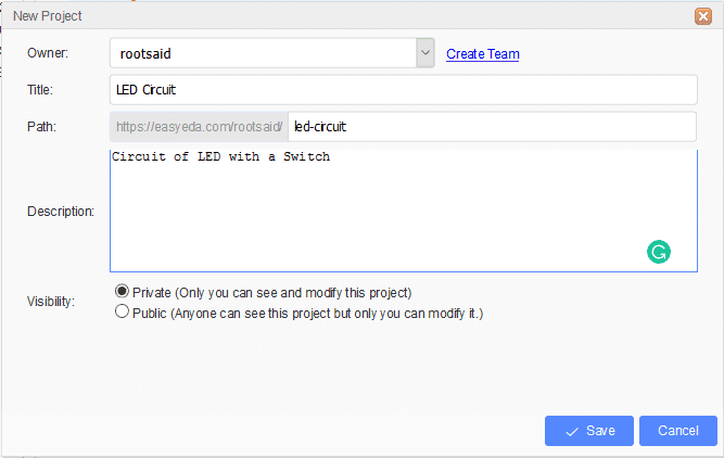
Step 2 : Start a New Project
Now we will start a new project and start drawing our circuit diagram. Once you are logged in, Go to “Editor”.

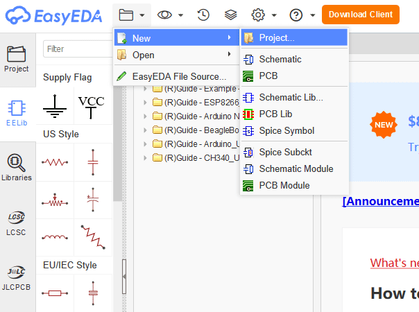
File -> New -> Project
Enter the Title, Path and Description and click on save button.

Once a new project is created, to modify your project, right-click on the folder with the project name in the project tree in the left-hand panel, which will open a web page in which you can edit your project.
Step 3: Draw the Circuit / Schematics
Pick and Place the components from the EELib tab from the left panel.

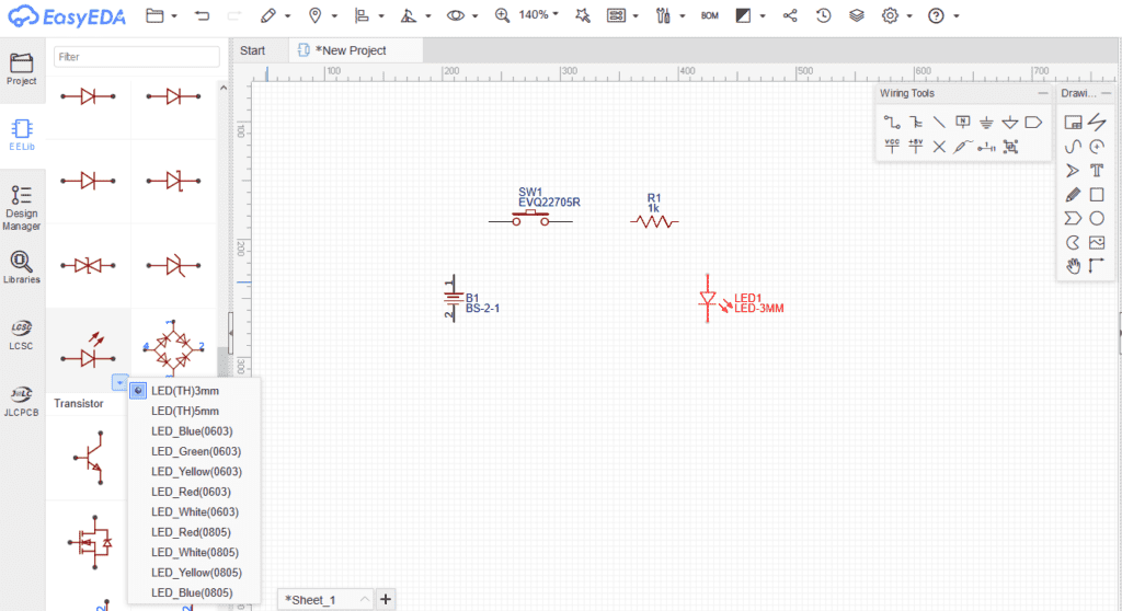
You can also go to libraries, and search for components there. Like I said before, EasyEDA has some cool and powerful drawing tools with which you can create your own symbols either by copying existing symbols into your own library and then editing and saving them, or by drawing them from scratch.
Use “Wire” tool to connect the components together.

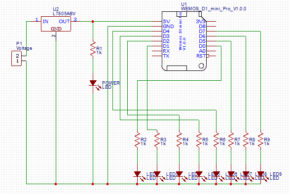
Step 4: Save the Schematics
Once you have finished drawing the circuit, save the circuit by clicking save.
Documents —> Save
Step 5 : Creating Online PCB Layout
Now, from the top tool list, Click on the convert button and select “Convert to PCB”.

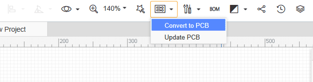
This will open up a window like this.

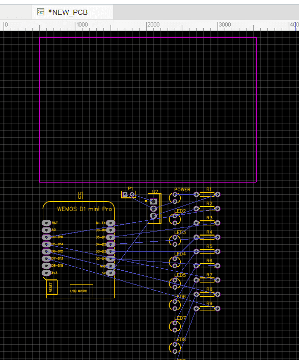
Step 6 : Placing the Components
Here, you can place the components inside the boundary and arrange them the way you want.
To make your PCB to look as clean as possible, It is best to place and route all components with the same function close to each other, like resistors for example.
Once you have finished placing all the components, click save.
Step 7 : Switching to 4 Layer
Now click the gear button on the Layers and Objects Tab. This will open up a window like this.

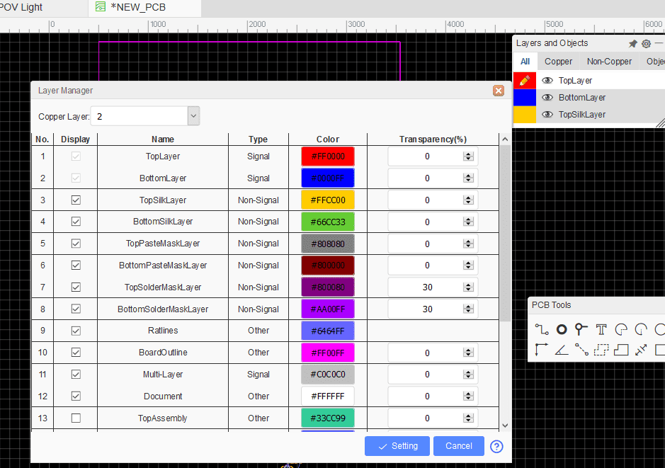
Here, click the “Copper Layer” drop box and select 4.

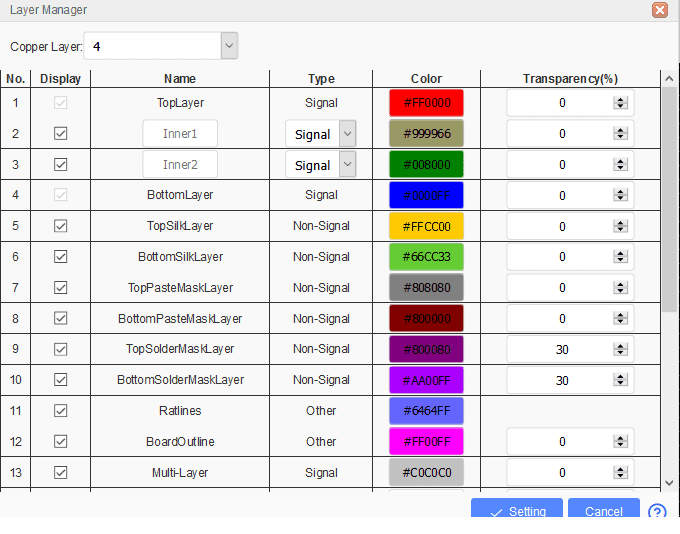
Once that is selected, click on Settings. You are done.
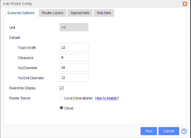
Step 8 : Routing the Components
For that, Click on the “Route” Tool and Select “Auto Router”
Now you can start routing all the components. The easy way route all the component is “auto-route” process.
From there click on “Router Layers” tab

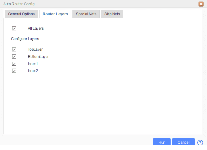
There, select all layers.
Go back to “General Options” where you can provide details such as clearance, track width, layer information etc. Once you have done that, click on “Run”.

Thats it guys, you layout is now complete. You can now download the Gerber file and use it to manufacture your PCB from JLCPCB.

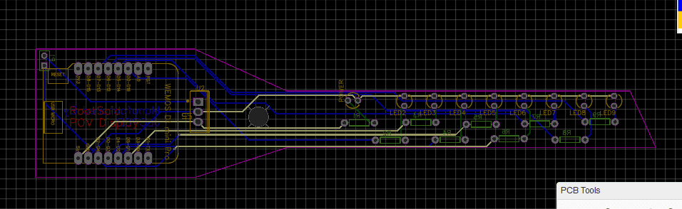

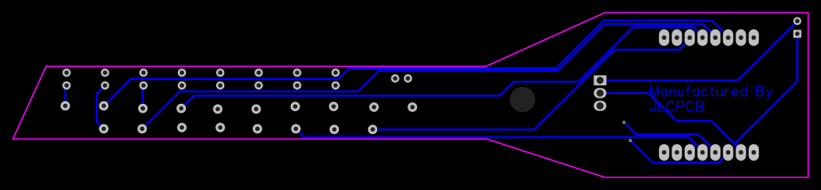
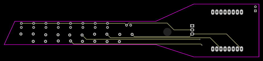
This is just a simple example for beginners to get started with. You can create multilayer, complex SMD circuits and get your PCB Layout neat and finished. in minutes.
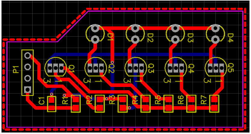
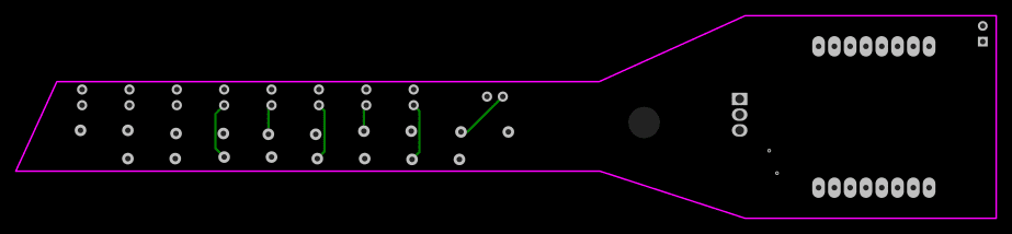
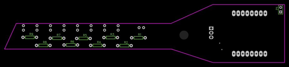
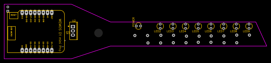
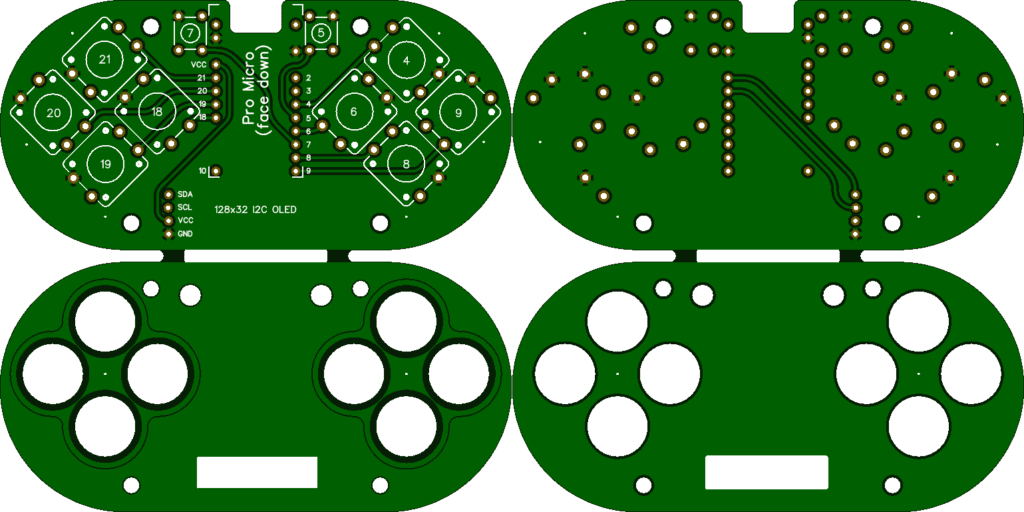
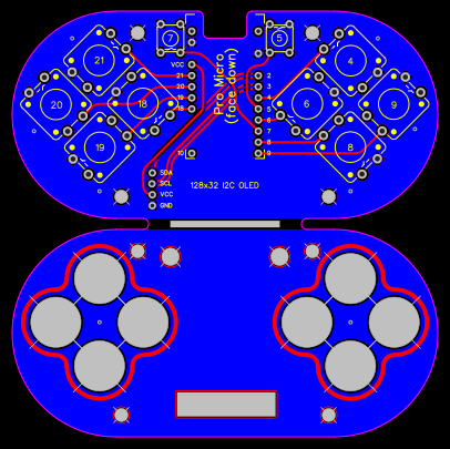
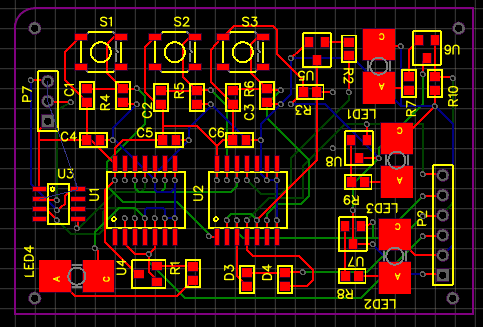
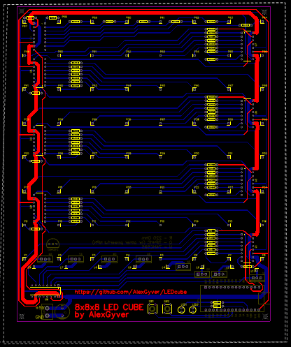
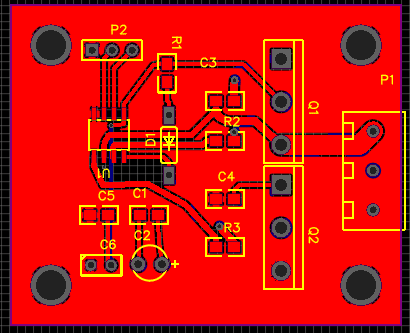
Shown below are some of the cool PCB Layouts Developed using EasyEDA


For more details, check out EasyEDA documentation.
[RICH_REVIEWS_FORM]
[RICH_REVIEWS_SNIPPET stars_only=”true”]
New to Robotics?
We have a beginners guide on “Getting Started with Robotics” which will give you a kick start in this field. Check out our free video tutorial below for a brief introduction.