AlYN/GaN: The Next-Gen Semiconductor Revolutionizing Energy-Efficient Electronics
Scientists at Fraunhofer IAF have made an important discovery in semiconductor materials. They’ve developed and tested a new material called aluminum yttrium nitride (AlYN) using a special process known as MOCVD.

AlYN has great potential because it has excellent properties and works well with gallium nitride (GaN). This makes it promising for use in energy-efficient, high-performance electronics, especially in information and communications technology.
What is MOCVD process?
Metal Organic Chemical Vapor Deposition (MOCVD) is a specialized form of Chemical Vapor Deposition (CVD) used primarily for creating crystalline micro and nano thin films and structures. This technique allows for precise control over the deposition process, enabling the creation of sharp, well-defined interfaces and fine modulation of the material’s properties. Additionally, MOCVD provides excellent control over the incorporation of dopants, which is crucial for tailoring the electrical and optical characteristics of the deposited layers.
MOCVD is crucial in producing high-performance electronic devices because it can create very pure and defect-free materials. It’s particularly important for making materials that are used in LEDs, lasers, and power electronics, where the quality of the semiconductor layers directly affects the performance and efficiency of the devices.
Aluminum Yttrium Nitride (AlYN) is emerging as a material with remarkable potential, making it a strong candidate for driving future technological advancements. Its unique material properties suggest that AlYN could play a crucial role in the next generation of electronic devices and systems.
Recent studies have already highlighted some of the impressive characteristics of AlYN, including its ferroelectric properties. These findings underscore the material’s suitability for various advanced applications. Researchers at Fraunhofer IAF have been particularly focused on how well AlYN can be integrated with gallium nitride (GaN).
One of the key benefits of AlYN is its ability to match GaN’s lattice structure almost perfectly. This compatibility between AlYN and GaN opens up new possibilities for creating AlYN/GaN heterostructures, which could offer significant advantages in developing cutting-edge electronics. This adaptability not only enhances the performance of devices but also paves the way for innovations that could shape the future of the electronics industry.
The Story
In 2023, Fraunhofer IAF researchers achieved a major milestone by depositing a 600 nm thick AlYN layer with over 30% yttrium concentration. They have since advanced further by fabricating AlYN/GaN heterostructures with up to 16% yttrium, showing excellent structural and electrical properties. Dr. Lutz Kirste’s team continues to explore the structural and chemical properties of AlYN, uncovering its promising potential for future applications.
Applications
High-frequency
Aluminum Yttrium Nitride (AlYN), with its wurtzite crystal structure, can be effectively matched to the wurtzite structure of Gallium Nitride (GaN) by carefully adjusting its composition. This compatibility makes AlYN a promising material for developing semiconductor components that offer enhanced performance and reliability. The ability to create a stable AlYN/GaN heterostructure opens up new possibilities for advanced electronic devices.
One of the most exciting aspects of AlYN is its ability to induce a two-dimensional electron gas (2DEG) within heterostructures. Recent research by Fraunhofer IAF has shown that AlYN/GaN heterostructures exhibit optimal 2DEG properties, particularly when the yttrium concentration is around 8%. This discovery highlights the potential of AlYN to significantly improve the efficiency of semiconductor devices.
Material characterization studies have further demonstrated that AlYN is well-suited for use in high electron mobility transistors (HEMTs). Researchers observed a notable increase in electron mobility at low temperatures, reaching more than 3000 cm²/Vs at 7 K. This finding is crucial for the development of high-performance HEMTs, and the research team has already made considerable progress in creating the necessary epitaxial heterostructures for these devices.
In terms of industrial applications, there is optimism surrounding the use of AlYN/GaN heterostructures on 4-inch SiC substrates. The successful growth of these heterostructures has demonstrated both scalability and structural uniformity, which are essential for commercial production. The ability to create AlYN layers using a commercial MOCVD reactor further supports the potential for scaling up to larger substrates in even bigger reactors.
This approach is regarded as one of the most efficient methods for producing large-area semiconductor structures, underscoring the potential of AlYN in the mass production of semiconductor devices. These advancements position AlYN as a material of significant interest for future electronic components, offering both high performance and the ability to be produced on a large scale.
Innovations in Non-Volatile Memory Design
First, it’s important to understand what ferroelectric materials are and why they are significant in the context of non-volatile memory. Ferroelectric materials are substances that exhibit spontaneous electric polarization (a separation of positive and negative charges) that can be reversed by the application of an external electric field.
This property is akin to how magnets have magnetic polarity, but here, it’s electric polarity. Non-volatile memory (NVM) refers to a type of memory that retains stored data even after the power is turned off. Examples include Flash memory, EEPROM, and emerging technologies like Ferroelectric RAM (FeRAM).
Why AlYN is Suitable for Non-Volatile Memory Applications
The ferroelectric nature of AlYN means it can maintain its polarization state even when the electric field is removed. This is critical for non-volatile memory because it allows data to be stored reliably without a continuous power supply. When a bit of data is written into memory, the polarization state of the AlYN layer can represent a binary ‘0’ or ‘1’. Since this state doesn’t change when the power is turned off, it ensures that data remains intact until it’s intentionally altered.
Another crucial advantage of AlYN is that it has no significant limitations on layer thickness. In many materials, the properties of thin films can degrade as the thickness changes, leading to instability in memory performance. However, AlYN does not suffer from these limitations, making it a versatile choice for memory fabrication. Whether the memory cells are required to be very thin for high-density storage or thicker for other design considerations, AlYN can maintain consistent performance.
Data centers are notorious for their high energy consumption, partly due to the vast amount of data they handle and the need to keep systems running continuously. The introduction of energy-efficient memory technologies, like those potentially based on AlYN, could help reduce this energy burden. Non-volatile memories that require less power to operate and retain data without continuous power input could make a substantial difference in the overall energy efficiency of data centers.
In the context of increasing global awareness of environmental impact, finding ways to reduce the energy footprint of data centers is crucial. AlYN-based memories, with their potential for lower power consumption and high efficiency, align well with these sustainability goals. By integrating such technologies, data centers can help mitigate their environmental impact while meeting the growing demands for data processing and storage.
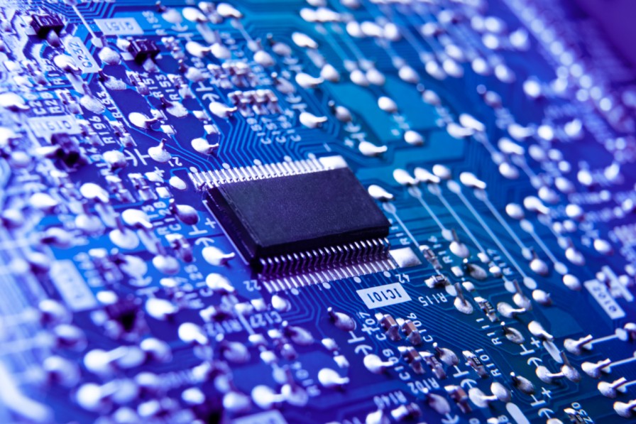
High Quality PCBs with PCBWay
PCBWay is a prominent name in the electronics manufacturing industry, known for providing high-quality printed circuit board (PCB) prototyping, manufacturing, and assembly services. With a reputation for precision and reliability, PCBWay has become a go-to solution for engineers, hobbyists, and companies alike, who need custom PCBs for a wide range of applications. Their services cover everything from simple single-layer boards to complex multi-layer designs, offering quick turnaround times and competitive pricing.


PCBWay’s commitment to quality extends to their assembly services, where they provide comprehensive support, including surface-mount technology (SMT), through-hole technology (THT), and mixed assembly processes. This makes PCBWay a one-stop shop for bringing innovative electronic designs to life, catering to the growing demands of the global electronics market. Whether you’re working on a small prototype or a large-scale production run, PCBWay ensures that your PCB needs are met with expertise and efficiency.
Conclusion
In conclusion, the emergence of Aluminum Yttrium Nitride (AlYN) as a new semiconductor material holds tremendous promise for the future of electronics. Its unique ferroelectric properties and ability to perform consistently across varying layer thicknesses make it an ideal candidate for developing more energy-efficient and powerful devices. As the demand for higher performance and sustainability in electronics continues to rise, AlYN’s potential to drive innovation in memory technologies and beyond cannot be overstated. By enabling more efficient data storage and processing, AlYN could play a pivotal role in shaping the next generation of electronics, paving the way for a future where advanced technology meets environmental responsibility.