Stop Failing Your Projects: 7 Common PCB Design Mistakes You’re Making Right Now!
Avoid These 7 Common PCB Design Mistakes!
Introduction
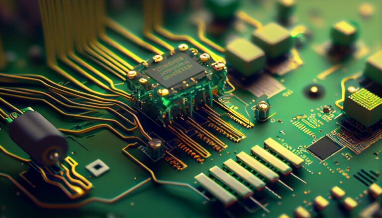
Imagine you’re building the backbone of any electronic device – the Printed Circuit Board (PCB). These marvels are crucial but can be daunting, especially for beginners. From my early days of squinting at tiny resistors to navigating complex software, I’ve learned that simple missteps in PCB design can lead to frustrating setbacks. This article will explore common PCB design mistakes and how to sidestep them to keep your electronics projects buzzing along smoothly!
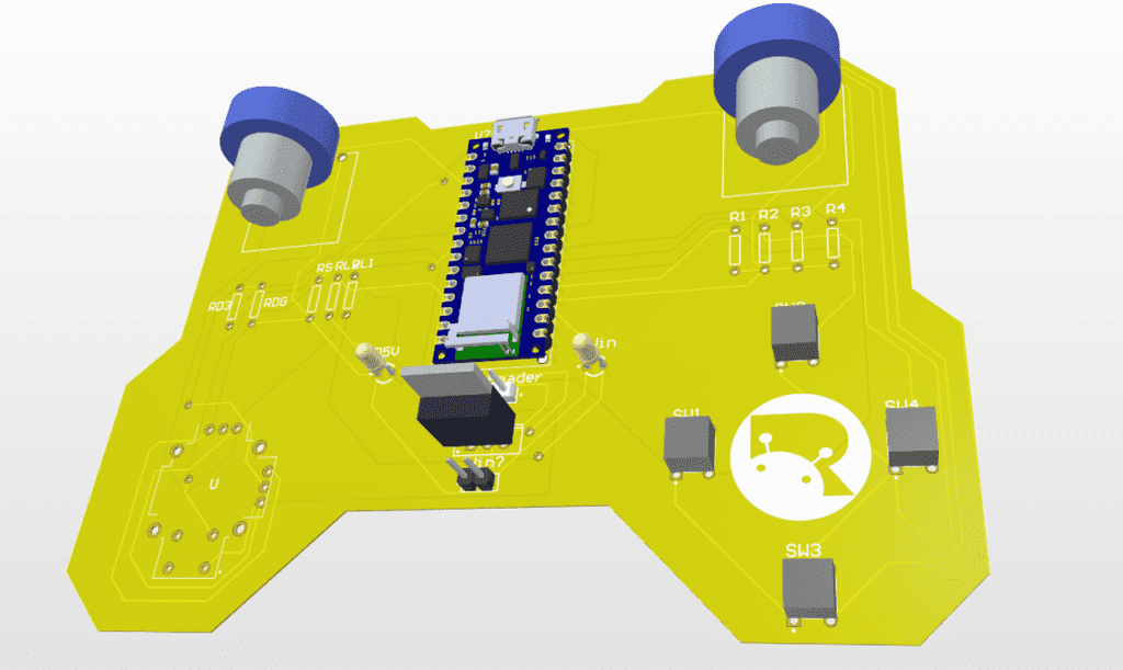
1. Overlooking the Importance of Proper Component Placement
Remember playing Tetris? Designing a PCB feels a bit like that, but each block (or component) can dramatically impact the entire game (your circuit functionality and signal integrity). In one of my first projects, I placed a high-frequency component too close to others, which led to annoying interference.


Tips for Optimizing Placement:
- Group Related Components: Just like keeping your spices near the stove, place related components together to simplify connections.
- Minimize Path Lengths for Critical Signals: Keep critical paths short and direct. This reduces the risk of signal loss or interference, much like using a shortcut on your daily commute!
2. Ignoring Power and Ground Plane Integrity
Have you ever witnessed lights flickering at home during a storm? Similar disturbances can happen in your PCB if power and ground planes aren’t designed carefully. Known as ground bounce and power integrity issues, they can make or break your circuit’s performance.
Strategies to Strengthen Planes:
- Proper Layer Allocation: Ensure adequate allocation for power and ground layers to stabilize voltage levels across the board.
- Decoupling Capacitors: These are your circuit’s ‘shock absorbers’, helping to smooth out unwanted voltage spikes.
3. Neglecting Trace Width and Spacing Rules
Choosing the width and spacing of traces on your PCB is somewhat akin to selecting pipes for plumbing. Too narrow, and you risk congestion and overheating. I once designed a board with inadequate trace width that literally smoked on initial power-up!
Guidelines:
- Understand Current Requirements: Trace width should accommodate the current passing through it. There are handy online calculators to help determine these measurements.
- Keep Safe Distances: Proper spacing helps prevent accidental shorts and reduces crosstalk between signals.
4. Insufficient Attention to Thermal Management
Anyone who’s touched a device that’s too hot to handle understands the discomfort thermal issues can cause. For PCBs, excessive heat can degrade or destroy electronic components.


Design Techniques for Better Heat Dissipation:
- Use Thermal Vias: These are essentially heat pipes in miniature, helping to move heat from one side of the board to the other or to a heat sink.
- Integrate Heat Sinks: Just like using fans to cool down a room, heat sinks help dissipate excess heat away from critical components.
5. Inadequate Design for Manufacturability (DFM)
Think of DFM like planning a party. Without considering the space and needs, you could end up with a cramped and uncomfortable environment. In PCB design, ignoring DFM principles can lead to boards that are difficult or impossible to manufacture at scale.
Tips for Enhancing Manufacturability:
- Simplify Shapes: Odd-shaped boards may seem cool but can complicate manufacturing and increase costs.
- Consider Component Density: High density may look efficient but can pose challenges in soldering and assembly. Balance is key!
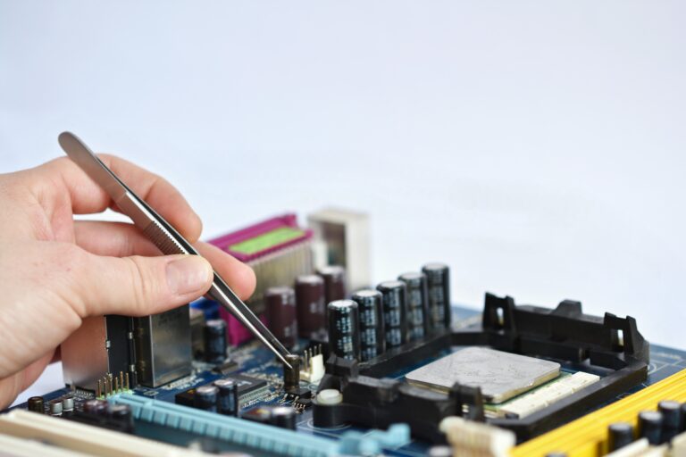
6. Not Testing the Design Thoroughly
Releasing a PCB design without thorough testing is like publishing a book without editing—risks abound. In my first circuit, a missed solder connection provided a memorable lesson on the importance of checking and rechecking.

Tools and Methods for Effective Testing:
- Software Simulation: Use programs to simulate your design’s behavior before building a physical prototype.
- Prototype Testing: Always build a prototype! It’s the best way to catch issues before full-scale production.
7. Forgetting to Review and Update Design Documentation
Documentation is the roadmap of PCB design, detailing every turn and stop. In the past, failing to update documentation led to a mismatch during assembly—a costly error.
Tips for Effective Documentation:
- Keep It Updated: As changes to the design occur, update all relevant documents to avoid confusion.
- Be Detailed: Clear, detailed documents can help ensure accuracy during manufacturing and assembly.
Conclusion
Avoiding these common mistakes in PCB design not only improves the performance and functionality of your boards but also saves time, costs, and headaches. Adopt a meticulous approach, keep learning from each project, and remember, in electronics, precision is everything.
Call to Action
Eager to sharpen your PCB design skills? Dive into online courses, engage with tutorials, and practice hands-on projects. Join forums or local electronics communities to exchange ideas and learn mutually. Remember, every mistake is a series of learning opportunities. Let’s design smarter, not harder!