Unlock the Secrets: Design Your First PCB in Just 24 Hours – Experts Can’t Believe It!
Introduction
Ever wondered how the little green boards inside your gadgets manage all their electronic wizardry? Those are printed circuit boards (PCBs), vital backbones of modern electronic devices. Learning PCB design not only demystifies how your tech operates but also empowers you to bring your own electronic projects to life. In this guide, I’ll walk you through designing your very first PCB in just 24 hours!


Getting Started with PCBs
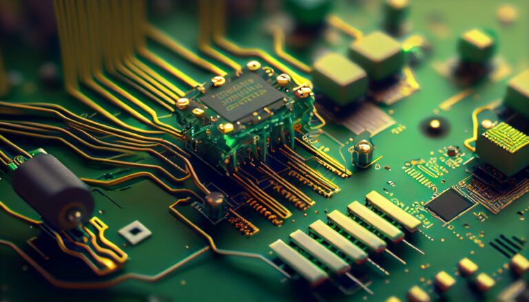
A PCB, or printed circuit board, is at the heart of nearly all electronic devices, providing connectivity and support to various components. It might sound complex—and it can be—but it’s also a skill anyone can learn. Remember my first venture into PCB design? I was determined to build a custom light timer but daunted by the idea of assembling my own PCB. Twenty-four hours later, I had a functional design ready for printing. If I can do it, you definitely can!
The process of creating a PCB involves several stages. Initially, a design layout is created using specialized software to map out the electrical connections and component placements. Once the design is finalized, it is transferred onto the copper-clad substrate. The unwanted copper is then removed, typically through a chemical etching process, leaving behind only the desired conductive tracks and pads. Additional layers of insulation and protective coatings are often applied to enhance the durability and reliability of the PCB.
Section 1: Understanding PCB Basics
Definition and Role of PCBs
A Printed Circuit Board (PCB) is a foundational component in modern electronic devices. It serves two primary functions: providing mechanical support for electronic components and facilitating electrical connections between them.


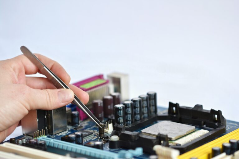
Mechanically, a PCB supports various electronic components, such as resistors, capacitors, transistors, and integrated circuits, by providing a stable and secure mounting surface. These components are typically attached to the PCB using solder, ensuring they remain in place even when the device is subject to physical movement or vibrations.
Electrically, a PCB connects these components through a network of conductive pads, tracks, and pathways. These conductive elements are meticulously designed and etched from copper sheets that are laminated onto a non-conductive substrate, usually made of materials like fiberglass, epoxy, or other composites. The copper tracks act as wires, creating specific electrical pathways that enable the flow of electricity between the different components.
Types of PCBs
- Single-sided (one copper layer),
- Double-sided (two copper layers),
- Multi-layer (more than two layers).
Components of a PCB
- Trace: Conductive paths for signal transmission.
- Pads: Anchoring points for components.
- Layers: Multiple stacked copper layers.
- Vias: Connective holes that link different layers.
- Silkscreen: Printed labels on the PCB for guidance.
Section 2: Necessary Tools and Materials
Software Tools
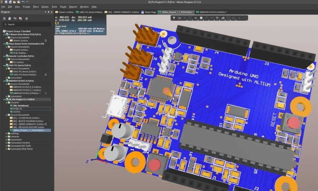
I recommend starting with user-friendly options like Altium, Eagle, or Fritzing for your PCB design projects. These tools are well-regarded for their ease of use and robust features, making them ideal for beginners. Each software has its own strengths: Altium is known for its comprehensive suite of tools and active support community, Eagle offers advanced capabilities and integration with Fusion 360, and Fritzing provides an intuitive interface perfect for educational purposes. For my first project, I chose Altium due to its straightforward interface, which makes it easier for newcomers to get started, and the active community that offers a wealth of tutorials and troubleshooting help.

Installation of these programs is generally straightforward, involving downloading the installer suited for your operating system and following the on-screen instructions. KiCad, for example, provides detailed installation guides on its website to help users through the process. Once installed, these tools open up a world of possibilities for designing and testing circuit boards. Whether you’re a hobbyist or an aspiring professional, starting with a user-friendly tool like KiCad, Eagle, or Fritzing can significantly smoothen your learning curve and enhance your project outcomes.
Hardware Needs
Ensure your computer meets the specifications for your software. You’ll also need basic electronic tools for later testing—things like a multimeter and soldering equipment.
Section 3: Planning Your PCB Design
Conceptualization
Define the purpose of your PCB. For my timer project, it was about controlling lights automatically. Deciding on the complexity (single vs. double-sided) should align with your project’s functionality.
Schematic Drawing
Draw your first schematic diagram using tools within your chosen software. Approach this task methodically, considering the schematic as a blueprint of your design. Each component you place on the schematic must be logically connected, ensuring that the overall structure accurately represents your intended design. This diagram serves as the foundation upon which your project will be built, making it essential to be thorough and precise in your connections. Pay close attention to detail and double-check each link between components to avoid errors.

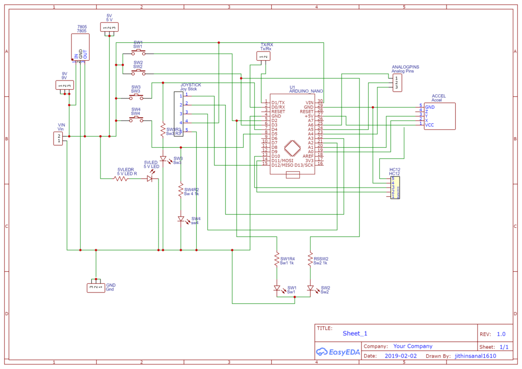
This step is crucial, as any mistake in the schematic can have a ripple effect, potentially compromising the entire design. An inaccurate or incomplete schematic can lead to malfunctioning circuits, increased troubleshooting time, and unnecessary rework. Therefore, take your time to verify the connections and ensure that all components are correctly placed and labeled. Properly documenting each part and its connections not only aids in the current design process but also serves as a valuable reference for future modifications and troubleshooting. By investing effort in creating an accurate and detailed schematic, you lay a solid foundation for a successful and efficient design process.
Section 4: Designing the PCB
Layout Design
Converting schematics to an actual PCB layout involves strategically placing components to minimize space and maximize functionality. This process requires careful consideration of each component’s placement to ensure optimal performance and reduce potential interference. Routing, which involves connecting components with traces, is akin to solving a complex puzzle.


It requires finding the most efficient paths for these connections while avoiding line crossings and ensuring signal integrity. The goal is to create a cohesive, functional design where every component works harmoniously within the limited space available on the PCB. This meticulous approach ensures the final product is both efficient and reliable.
Verification and Validation
Always check your design for errors to ensure a smooth and successful manufacturing process. Utilizing the Design Rule Check (DRC) feature in your PCB design software is essential. This tool acts like a second set of eyes, meticulously scanning your design for potential issues that might be overlooked during manual reviews. By leveraging DRC, you can identify and rectify errors early, saving time and resources while preventing costly mistakes. It’s a crucial step in maintaining high-quality standards and ensuring that your final product functions as intended.
Section 5: Preparing for Manufacturing
Generating Gerber Files
Once you’re confident in your design, the next crucial step is to export it as Gerber files. Gerber files are an industry-standard format used by PCB manufacturers to precisely understand and produce the layout of your printed circuit board. These files contain all the necessary information about the different layers of the PCB, such as the copper layers, solder mask, silkscreen, and drill data.

By converting your design into Gerber files, you ensure that every detail of your PCB design is accurately communicated to the manufacturer, enabling them to fabricate your board with the highest precision. This process is essential for translating your digital design into a physical product that meets your exact specifications.
Selecting a Manufacturer
Consider factors like cost, turnaround time, and reputation when choosing a manufacturer. Ordering a prototype can be exciting—as it was for me, receiving my first ever designed PCB was quite the thrill!
Section 6: Practical Tips for Success
Common Pitfalls and How to Avoid Them
Many beginners, including myself, often make the mistake of mismatched component footprints or incorrect trace sizing when creating their own PCBs. This common error arises from a lack of attention to detail and a misunderstanding of the importance of precise measurements. Mismatched footprints can lead to components that don’t fit properly on the board, causing assembly difficulties and potential functionality issues. Incorrect trace sizing, on the other hand, can result in inadequate current handling, leading to overheating or signal integrity problems. To avoid these pitfalls, it’s crucial to be meticulous in checking the specifications of each component and ensuring that the PCB design adheres to these requirements. Double-checking measurements, verifying compatibility, and understanding the electrical demands of your design are essential steps in producing a reliable and functional PCB.
Additional Resources
There are countless resources available—from books like “PCB Design for Real-World EMI Control” by Bruce Archambeault to online courses and communities. Engaging with these can enhance learning significantly.
Conclusion
In summary, a PCB is a critical element in electronic devices, providing both mechanical support and electrical connectivity through a sophisticated arrangement of conductive pathways and pads etched from copper sheets laminated onto a non-conductive base. This intricate design and manufacturing process ensures that electronic components are securely mounted and effectively interconnected, allowing for the proper functioning of the device.
There you have it—a beginner’s playbook to designing your first PCB in 24 hours. Remember, each design iteration teaches you something new. Use the vast resources available, experiment often, and don’t hesitate to ask for help.
Call to Action
Ready to start your first project? Dive in, design, and share your experiences in forums like Reddit’s r/PCB. Good luck, and have fun designing!
Appendix
Glossary of Terms
- PCB: Printed Circuit Board
- Trace: A continuous path in copper.
- Via: A hole in the PCB that connects different layers.
FAQs about PCB design for beginners
- What is the best software for beginners? Easy-to-learn platforms like Altium and Fritzing are ideal.
- Can I design a PCB on a regular home computer? Yes, but ensure it meets the minimum requirements of the software.
Embark on your PCB design journey today and transform those ideas into functional realities!