Designing PCBs for High-Speed Signals and Mixed-Signal Circuits
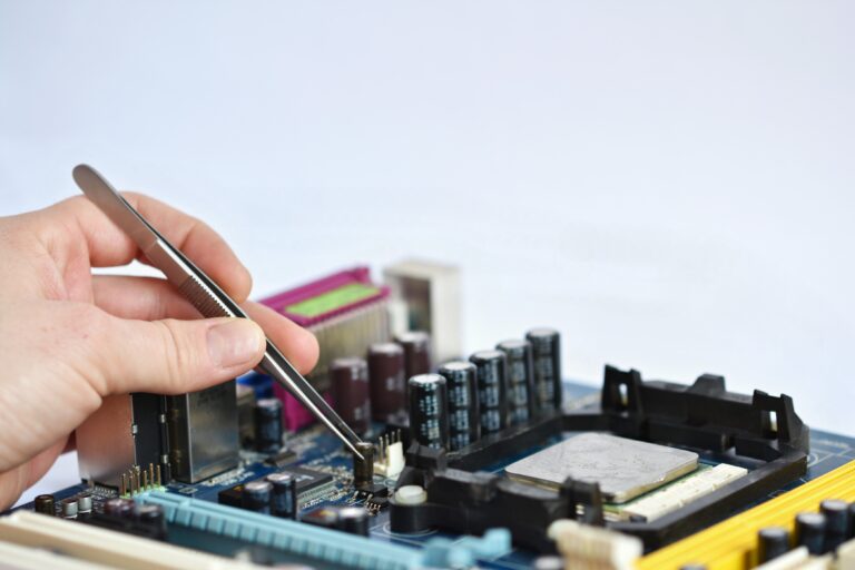
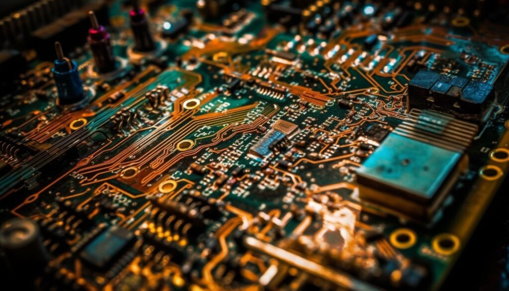
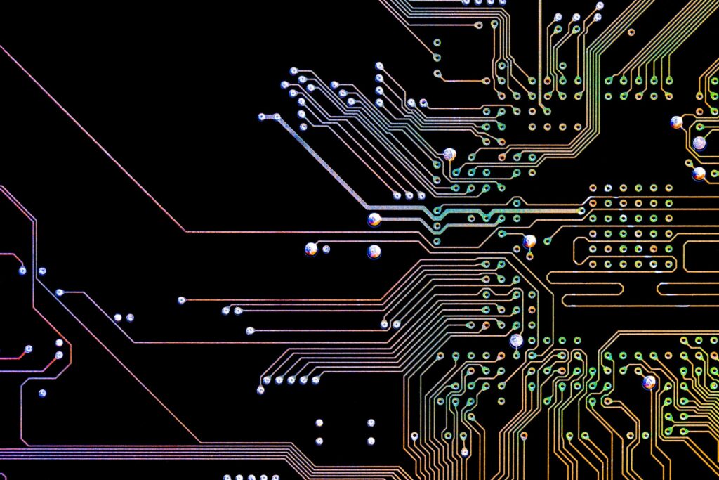
Every modern electronic system relies on Printed Circuit Boards (PCBs) as its core platform. As devices become faster, smaller, and more integrated, designers face unique challenges—especially when working with high-speed digital signals and mixed analog/digital circuits. Careful planning and layout are critical to ensure performance, reliability, and manufacturability.

In this blog, we’ll explore High-Speed PCB Design Guidelines, share essential Mixed-Signal PCB Design Best Practices, and explain why Signal Integrity in High-Speed PCB Design is more important than ever.
High-Speed PCB Design Guidelines
When dealing with components such as DDR memory, microprocessors, and gigabit transceivers, PCB traces no longer behave like simple wires—they act as transmission lines. Following structured high-speed PCB design guidelines helps avoid issues like signal reflections, EMI, and timing errors.
Key considerations include:
- Controlled Impedance Routing: Keep differential pair traces (e.g., USB, HDMI, Ethernet) matched in length and width to maintain impedance.
- Ground Planes: Always use solid reference planes to provide return paths and reduce loop inductance.
- Via Management: Minimize via count on high-speed paths to reduce discontinuities. Blind or microvias can help.
- Length Matching: For parallel buses (e.g., DDR data lines), match trace lengths to avoid skew between signals.
By adhering to these guidelines, designers can maintain predictable performance and reduce costly re-spins.
Mixed-Signal PCB Design Best Practices
Most real-world electronics are mixed-signal boards—combining analog (sensors, amplifiers, ADCs/DACs) with digital (microcontrollers, logic circuits). Without proper layout strategies, digital switching noise can corrupt sensitive analog signals.

Here are some proven mixed-signal PCB design best practices:
- Partition Layouts: Separate the analog and digital domains on the PCB to minimize interference. Place components according to their signal domain.
- Ground Strategy: Use a single, continuous ground plane but carefully route return currents to prevent digital noise coupling into analog areas.
- Power Decoupling: Add bypass capacitors close to IC power pins to suppress noise.
- Shielding Sensitive Traces: Route analog traces away from clock lines, switching regulators, and high-speed buses.
By following these practices, designers can achieve clean analog performance while maintaining digital functionality.
Signal Integrity in High-Speed PCB Design
At higher frequencies, the integrity of electrical signals becomes the deciding factor for system performance. Poor signal integrity in high-speed PCB design can lead to jitter, data loss, and functional failure.
To preserve signal quality:
- Minimize Crosstalk: Increase spacing between high-speed traces and route differential pairs tightly coupled.
- Proper Termination: Use series or parallel termination to eliminate reflections on long traces.
- Avoid Stubs: Keep test pads and unused vias off high-speed traces to prevent unwanted resonances.
- Simulate Early: Use signal integrity simulation tools to verify layout decisions before fabrication.
Strong SI practices ensure that signals arrive clean and undistorted, which is vital in applications like networking, automotive electronics, and industrial systems.
High-Speed Signal Integrity Challenges and Solutions
High-speed digital signals (such as fast clock lines, high-speed serial interfaces, or DDR memory buses) introduce a range of signal integrity challenges. As edge rates and frequencies increase, PCB traces behave like transmission lines, and designers must control parameters like characteristic impedance, minimize reflections, limit crosstalk, and manage signal timing (skew and jitter).
Common issues in high-speed boards include signal distortion due to impedance mismatch, reflections causing ringing, excessive insertion loss on long traces, and crosstalk between adjacent lines. These problems can lead to data errors or device malfunctions if not addressed. To mitigate such issues, designers use techniques like controlled impedance routing, proper termination, differential signaling, and trace length matching for timing alignment.

Modern PCB design tools provide invaluable help in implementing these techniques. For example, Altium Designer includes an integrated Layer Stack Manager that lets you configure your board’s layer stack-up and materials in order to achieve controlled impedance for high-speed traces. By setting up the dielectric layer thicknesses and copper weights, you can define target impedance profiles (e.g. 50 Ω microstrip lines or 90 Ω differential pairs), and the software will automatically calculate the required trace widths and clearances to meet those impedance goals.
In fact, Altium Designer leverages a built-in field solver (from Simberian) to precisely determine impedance based on the PCB stack-up geometry and materials. This means you can instantly determine the PCB trace width needed to hit your target impedance in the board design phase. With a correct stack-up and impedance profile in place, every high-speed route you lay out in Altium can adhere to the impedance requirements by design.
Conclusion
Designing PCBs for high-speed signals and mixed analog/digital boards requires a blend of physics, engineering discipline, and practical experience. By applying High-Speed PCB Design Guidelines, respecting Mixed-Signal PCB Design Best Practices, and prioritizing Signal Integrity in High-Speed PCB Design, engineers can deliver reliable, high-performance boards.
Whether you’re a professional PCB designer, a hobbyist working on your first mixed-signal project, or an engineering student learning advanced techniques, these principles will help you create designs that work the first time—and every time.