The Ultimate Beginner’s Guide to PCB Design: Start Here!
Welcome to the fascinating world of PCB (Printed Circuit Board) design! If you’re new to electronics and eager to dive into PCB design, you’ve come to the right place. As an experienced electronics engineer specializing in PCB design, I’m here to guide you through the essential steps, tips, and tools you need to get started. Let’s embark on this journey together!
Understanding the Basics
What is a PCB (Printed Circuit Board)?
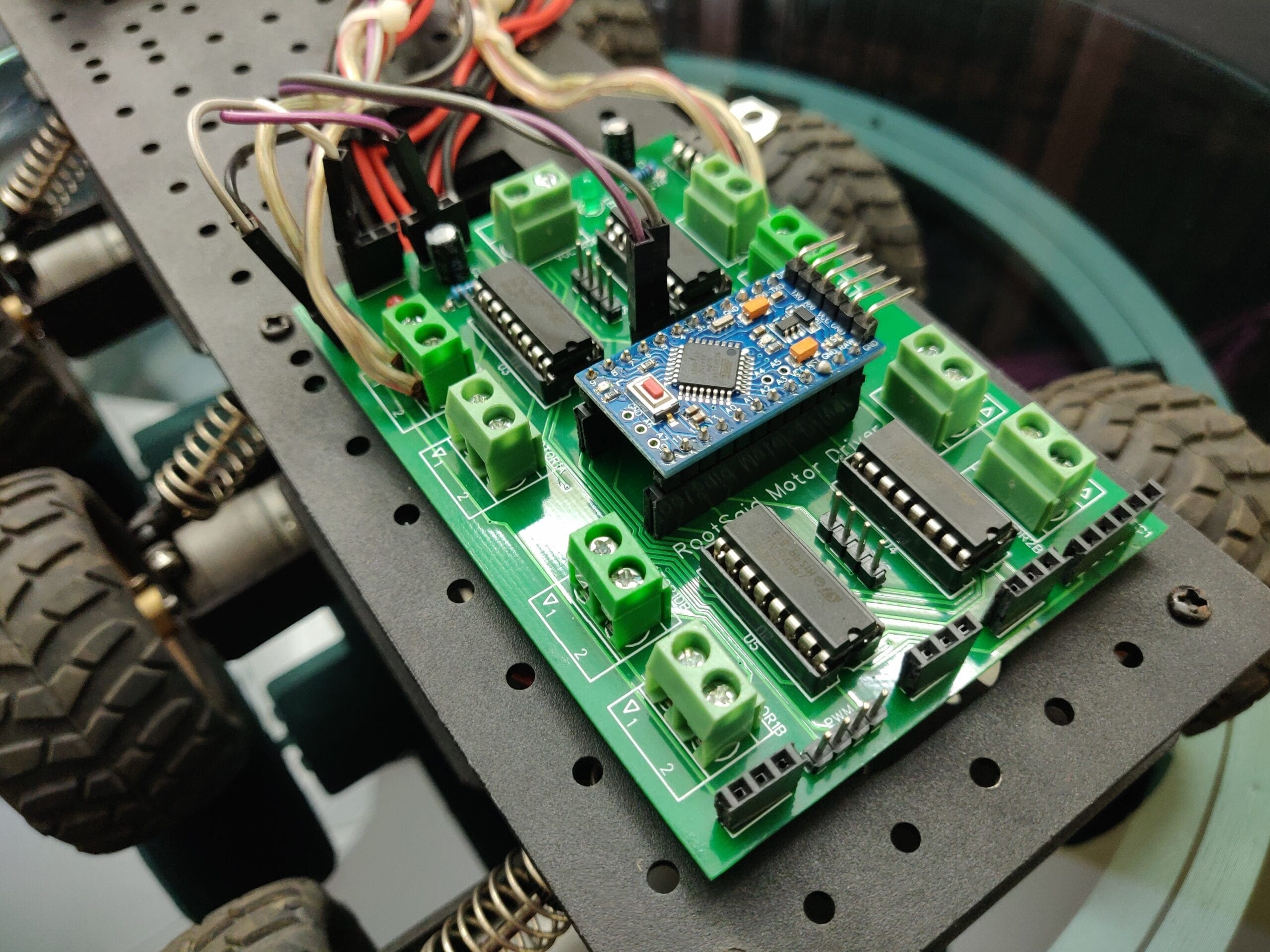
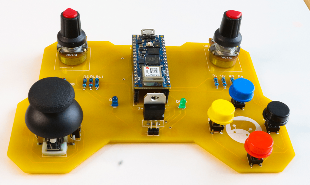
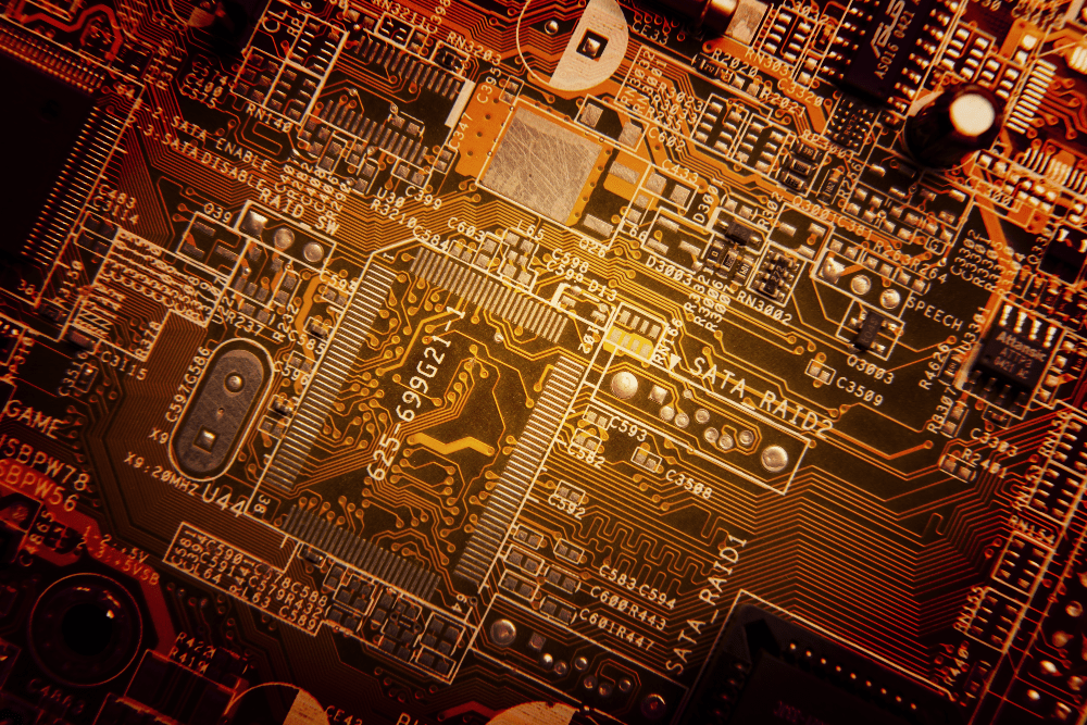
A PCB, or Printed Circuit Board, is the backbone of most electronic devices. It’s the board that physically supports and electrically connects the electronic components using conductive pathways, traces, and pads. Think of it as the “nervous system” of your gadget, directing electrical signals where they need to go.

When I first started in electronics, I was amazed at how a simple-looking board could hold the key to making complex devices work. The magic happens in those intricate pathways and connections.
Key Components of a PCB
Understanding the fundamental parts of a PCB will help you design better. Here are the main components:
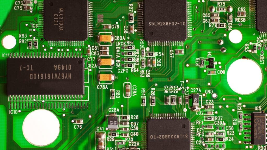
- Traces: The thin lines of conductive material (usually copper) that connect different components.
- Pads: The small areas of copper where components are soldered.
- Vias: The holes that allow traces to pass from one layer of the board to another.
- Silkscreen: The layer that displays printed information like component labels and symbols.
- Solder Mask: The protective layer that prevents solder from sticking to unwanted areas.
Each component plays a crucial role in ensuring your PCB functions correctly. For instance, when I worked on my first PCB project, I underestimated the importance of proper trace width, leading to overheating issues. Lesson learned!
Essential Tools and Software
Software for PCB Design
Choosing the right software is vital for your success. Here are some popular options:
- Altium Designer: A professional tool with extensive features, best suited for complex designs.
- Eagle: Great for beginners with a user-friendly interface.
- KiCad: Open-source and packed with features, making it ideal for both beginners and advanced users.
When I started, I used Eagle because of its straightforward interface and helpful community. It made my learning curve much less steep.
Hardware Tools
You’ll need some basic tools to bring your designs to life:


- Soldering Iron: For soldering components onto the PCB.
- Multimeter: To check electrical connections and troubleshoot.
- Wire Cutters: Essential for trimming excess leads from components.
Creating a clean and organized workspace is also crucial. I remember setting up my first workstation on my bedroom desk, cluttered with wires and tools. It wasn’t ideal, but it got the job done. Over time, I realized the importance of keeping things tidy to avoid mistakes.
The Design Process
Step-by-Step Workflow
This beginner’s guide to PCB design involves several steps. Here’s a simplified workflow to get you started:
Schematic Design
Start by creating a schematic diagram, which is a blueprint of your circuit. It shows how components are connected without worrying about their physical placement. Most PCB design software includes a schematic editor.

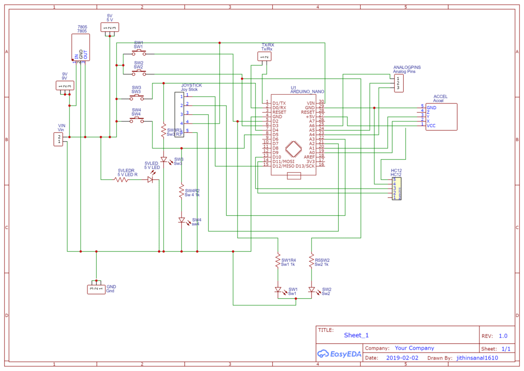
When I designed my first PCB, I skipped this step, thinking I could keep everything in my head. Big mistake! The schematic is your roadmap and helps prevent errors.

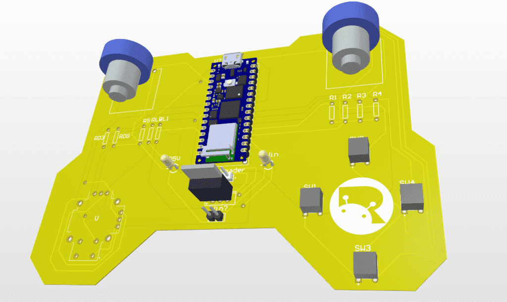
Component Placement
Once your schematic is ready, it’s time to place your components on the PCB layout. Here are some tips:
- Keep related components close to minimize trace length.
- Place larger components first, then fit smaller ones around them.
- Ensure there’s enough space for routing traces.
Proper placement is critical. In one of my early projects, I crammed everything too tightly, leading to difficult soldering and potential short circuits.
Routing Traces
Routing is the process of connecting the components with traces. Here are some principles to follow:
- Keep traces as short as possible to reduce resistance.
- Avoid sharp angles; use 45-degree angles instead.
- Ensure traces are wide enough to handle the current they will carry.
Routing can be challenging, but with practice, you’ll get better at it. I used to struggle with this, often ending up with spaghetti-like traces. Over time, I learned to plan my routes more efficiently.
Design Rules Check (DRC)
Before finalizing your design, run a Design Rules Check (DRC) to catch potential issues. This automated check ensures your design complies with manufacturing capabilities and avoids common mistakes.
Ignoring DRC led to a few of my boards being rejected by manufacturers. Running DRC is a simple yet crucial step to save time and money.
Practical Tips for Beginners
Design Considerations
Here are some essential considerations to keep in mind:
- Power Integrity: Ensure stable power delivery to all components.
- Signal Integrity: Minimize interference and signal degradation.
- Thermal Management: Plan for heat dissipation, especially in high-power circuits.
I learned about thermal management the hard way when a board overheated and failed during testing. Adding heat sinks and considering airflow can make a big difference.
Common Mistakes to Avoid
- Overlooking Design Rules: Always follow the guidelines provided by your software and manufacturer.
- Poor Component Placement: Think ahead about how you’ll route traces.
- Inadequate Trace Width: Ensure your traces can handle the expected current.

Avoiding these mistakes will save you from headaches and costly revisions. Trust me; I’ve made them all!
Best Practices
- Keep it Simple: Start with basic designs and gradually tackle more complex projects.
- Save Regularly: Use version control to keep track of changes.
- Use Libraries: Take advantage of pre-made components to save time and reduce errors.
Starting simple helped me build confidence and skills. My first few boards were basic LED circuits, but they laid the groundwork for more advanced designs.
From Design to Production
Prototyping
Creating a prototype is a crucial step before full-scale production. You can prototype in-house if you have the tools or use third-party services.
For my first prototype, I used a local service. Seeing my design come to life was exhilarating. It also allowed me to catch and fix issues before moving to mass production.
Manufacturing Process
When you’re ready for production, prepare Gerber files, which are the standard format for PCB manufacturing. Choose a reliable manufacturer and understand their fabrication process.
Sending my first board to a manufacturer was nerve-wracking. I triple-checked everything but still encountered minor issues. Communication with your manufacturer is key to ensuring a smooth process.
Testing and Troubleshooting
Initial Testing
Once you receive your PCB, perform initial testing:
- Visual Inspection: Check for obvious defects or solder bridges.
- Electrical Testing: Use a multimeter to check for continuity and proper connections.
I vividly remember the excitement of testing my first board. I also remember the frustration of finding a short circuit that took hours to locate. Patience and thoroughness are crucial.
Debugging Common Issues
- Shorts and Opens: Use a multimeter to identify and fix these issues.
- Component Placement: Double-check that all components are correctly oriented and placed.
- Signal Integrity: Use an oscilloscope to identify and resolve signal problems.
Debugging can be frustrating, but it’s a valuable learning experience. Each problem you solve makes you a better designer.
Resources for Further Learning
Books and Online Courses
To deepen your knowledge, here are some excellent resources:
- Books: “The Art of Electronics” by Paul Horowitz and Winfield Hill is a classic.
- Online Courses: Platforms like Coursera and Udemy offer comprehensive PCB design courses.
I’ve found that combining books with hands-on projects accelerates learning. The Art of Electronics was a game-changer for me.
Community and Support
Join forums and online communities to connect with other PCB enthusiasts:
- Reddit: Subreddits like r/PrintedCircuitBoard and r/ECE provide valuable insights and support.
- Stack Exchange: Electronics Stack Exchange is great for asking questions and getting expert answers.
Engaging with the community helped me solve many tricky problems and stay motivated.
Conclusion
Recap and Encouragement
We’ve covered the basics of PCB design, from understanding components to prototyping and testing. Starting with simple projects, using the right tools, and learning from mistakes are keys to success.
Next Steps
As you gain confidence, move on to more complex designs and stay updated with the latest trends in PCB technology. Continuous learning and experimentation are the heart of electronics.