10 PCB Design Secrets You Wish You Knew Earlier!
Introduction
Hey there, budding electronics engineer! I’m excited to share some insider PCB design secrets with you. I’ve been in the electronics field for over a decade, specializing in PCB designing, and I’ve picked up quite a few tricks along the way. Whether you’re just starting out or looking to refine your skills, these tips will help you avoid common pitfalls and create better, more reliable PCBs.
Secret 1: Start with a Clear Schematic
Importance of a Clear Schematic
A solid PCB design starts with a well-organized schematic. Think of the schematic as the blueprint for your PCB. It’s crucial to ensure every connection and component is clearly laid out.


Tips for Creating a Clear Schematic
- Label Everything: Make sure every component and connection is clearly labeled. It’s easy to overlook something when you’re deep into the design process.
- Use Standard Symbols: Stick to standard symbols for components. This makes your schematic easier to read and understand, both for you and anyone else who might work on your project.
- Keep It Tidy: Organize your schematic neatly. Group related components together and avoid crossing wires whenever possible.
Personal Anecdote When I first started designing PCBs, I neglected the importance of a clear schematic. My first project was a mess of wires and labels, and I spent more time troubleshooting than designing. Since then, I’ve made it a rule to keep my schematics clean and organized. Trust me, it saves a lot of headaches down the road!
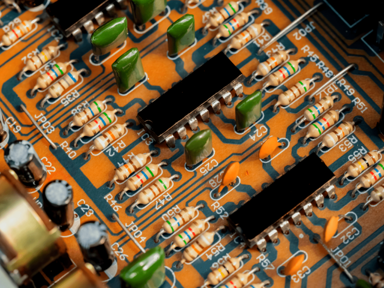
Secret 2: Component Placement is Key
Strategic Component Placement
Where you place your components can make or break your PCB design. Proper placement affects performance, signal integrity, and manufacturability.
Tips for Optimal Component Placement
- Start with High-Pin Components: Place components with the most pins first. This makes it easier to route your traces later.
- Consider Signal Path: Place components to minimize the length of critical signal paths. This helps reduce noise and signal degradation.
- Keep Power and Ground Planes Clean: Ensure power and ground connections are short and direct. This helps maintain signal integrity and reduces noise.

Examples of Good and Bad Placements Good placement involves grouping related components and keeping signal paths short. Bad placement, on the other hand, might involve scattered components and long, winding signal paths that introduce noise and interference.
Secret 3: Understand and Use Design Rules
Importance of Design Rules
Design rules are your best friend in PCB design. They ensure your board is manufacturable and meets all necessary specifications.
Setting and Customizing Design Rules Most PCB design software allows you to set and customize design rules. Take the time to familiarize yourself with these settings and tailor them to your project’s needs.
Common Design Rules
- Clearances: Ensure adequate spacing between traces to prevent short circuits.
- Trace Widths: Use appropriate trace widths for different current levels.
- Via Sizes: Select via sizes that are suitable for your board’s requirements.
Personal Anecdote I once ignored a design rule about trace widths and ended up with a board that couldn’t handle the current load. It was an expensive mistake that could have been avoided with proper adherence to design rules. Now, I always double-check my design rules before finalizing a project.
Secret 4: Optimize Your Trace Widths
Choosing the Right Trace Widths
Trace widths are crucial for the performance and reliability of your PCB. They need to be wide enough to handle the current but not so wide that they waste space.

Calculating Appropriate Trace Widths There are online calculators available to help you determine the right trace widths based on current load and other factors. These tools are invaluable for ensuring your traces can handle the required current.
Tools and Resources
- Online Trace Width Calculators: Use tools like the one from PCB Toolkit to calculate trace widths.
- Design Software: Many PCB design programs have built-in tools for trace width calculation.
Secret 5: Pay Attention to Signal Integrity
Understanding Signal Integrity
Signal integrity refers to the quality of the electrical signals on your PCB. Poor signal integrity can lead to malfunctioning boards and unreliable performance.
Maintaining Signal Integrity
- Minimize Crosstalk: Keep high-speed signal traces away from each other to avoid crosstalk.
- Use Ground Planes: Implement solid ground planes to provide a return path for signals and reduce noise.
- Avoid Right Angles: Route traces with smooth curves or 45-degree angles to minimize signal reflection.
Common Issues and Troubleshooting If you’re experiencing signal integrity issues, look for signs of crosstalk, signal reflections, and noise. Using an oscilloscope can help identify and troubleshoot these problems.
Secret 6: Proper Grounding Techniques
Importance of Grounding
A solid ground plane is essential for a stable and reliable PCB. It helps reduce noise and provides a reference point for signals.
Best Practices for Grounding
- Use a Continuous Ground Plane: Ensure your ground plane is continuous and covers as much of the board as possible.
- Minimize Ground Loops: Avoid creating ground loops, which can introduce noise and interference.
- Connect Grounds Correctly: Make sure all ground connections are short and direct.
Secret 7: Use Vias Wisely
Role of Vias in PCB Design
Vias are used to connect different layers of a PCB. Proper via placement and usage are crucial for maintaining signal integrity and ensuring manufacturability.

Effective Via Placement and Usage
- Minimize Via Count: Use the fewest number of vias necessary to reduce complexity and cost.
- Consider Via Sizes: Use appropriate via sizes for different signal types and current levels.
- Avoid Via in Pads: Avoid placing vias in component pads unless absolutely necessary, as this can complicate assembly.
Types of Vias
- Through-Hole Vias: Connect all layers of the PCB.
- Blind Vias: Connect an outer layer to one or more inner layers.
- Buried Vias: Connect inner layers without reaching the outer layers.
Secret 8: Thermal Management
Managing Heat in PCB Design
Heat management is critical for ensuring the reliability and longevity of your PCB. Excessive heat can damage components and affect performance.
Techniques for Thermal Management
- Use Thermal Vias: Implement thermal vias to dissipate heat from hot components.
- Add Heat Sinks: Attach heat sinks to high-power components to help dissipate heat.
- Conduct Thermal Analysis: Use thermal analysis tools to identify hotspots and optimize your design for better heat distribution.
Personal Anecdote In one of my earlier projects, I overlooked thermal management and ended up with a board that overheated and failed during testing. Since then, I’ve made it a point to always consider thermal management in my designs. It’s a small step that can make a huge difference in the reliability of your board.
Secret 9: DFM (Design for Manufacturability)
Overview of DFM
Design for Manufacturability (DFM) ensures your PCB can be manufactured efficiently and cost-effectively. DFM considerations can help avoid production issues and reduce costs.
Tips for DFM
- Standardize Component Sizes: Use standard component sizes to simplify assembly.
- Optimize Trace and Space Widths: Ensure traces and spaces are within manufacturable limits.
- Check for Solder Mask Slivers: Avoid thin strips of solder mask that can peel off during manufacturing.
Common DFM Considerations
- Hole Sizes: Use standard hole sizes for vias and through-hole components.
- Component Spacing: Ensure adequate spacing between components for assembly and soldering.
- Silkscreen Placement: Place silkscreen labels away from pads and traces to avoid interference.
Secret 10: Testing and Validation
Importance of Testing
Thorough testing is essential to ensure your PCB design works as intended. Testing helps identify and fix issues before the board goes into production.
Different Testing Methods and Tools
- Automated Optical Inspection (AOI): Uses cameras to inspect the board for defects.
- In-Circuit Testing (ICT): Tests individual components on the board for functionality.
- Functional Testing: Tests the complete board in its operational environment.
Setting Up a Test Plan Create a comprehensive test plan that includes all necessary tests and validation steps. Ensure you have the right tools and equipment to carry out these tests effectively.
Personal Anecdote In one of my projects, we rushed through testing and ended up with a batch of faulty boards. The experience taught me the importance of thorough testing and validation. Now, I always make sure to allocate sufficient time and resources for this critical step.
Conclusion
Recap of the 10 PCB design secrets shared in the article:
- Start with a Clear Schematic
- Component Placement is Key
- Understand and Use Design Rules
- Optimize Your Trace Widths
- Pay Attention to Signal Integrity
- Proper Grounding Techniques
- Use Vias Wisely
- Thermal Management
- DFM (Design for Manufacturability)
- Testing and Validation
Final Tips for Beginners Remember, PCB design is both an art and a science. It takes practice and continuous learning to master. Apply these PCB design secrets in your projects, and you’ll be well on your way to creating reliable, high-performance PCBs.
By mastering these PCB design secrets, you’ll not only improve the quality and reliability of your designs but also gain several key benefits:
1. Enhanced Efficiency: Understanding these secrets will streamline your design process, allowing you to create PCBs more quickly and with fewer errors.
2. Cost Savings: By optimizing your design for manufacturability and avoiding common mistakes, you’ll reduce production costs and minimize the need for costly revisions.
3. Improved Performance: Implementing these advanced techniques will enhance the performance and durability of your PCBs, ensuring they meet and exceed industry standards.
4. Competitive Edge: Knowledge of these insider tips will set you apart from your peers, making you a more valuable asset in any engineering team or project.
5. Future-Proof Designs: Stay ahead of the curve by incorporating the latest trends and best practices in PCB design, ensuring your projects remain relevant and effective.
Embrace these PCB design secrets and watch your skills and projects soar to new heights!