Tips for Choosing PCB Components
Important Tips for Choosing PCB Components
In choosing the appropriate PCB components that can bring your PCB design to fruition, there are some essential tips you should put into critical consideration. These tips are to be considered during the design process to make you derive an exotic PCB that will serve your needs.

The following tips will help you achieve a high PCB that will meet your customers’ specifications and needs.
1. Select components in the design stage
The PCB design stage should be the stage where you select PCB components because your design will determine the appropriate parts to choose from the market.
Therefore, you should choose a design that captures the height, width, and other properties of the component you want to use.

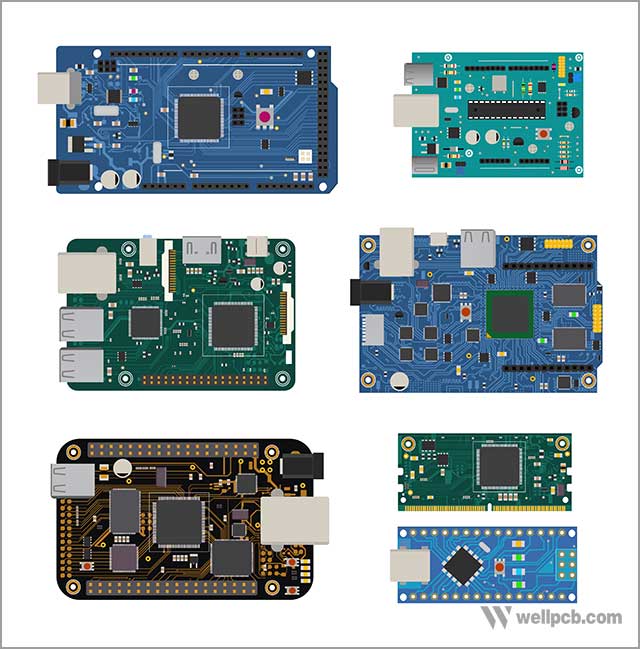
2. Consider the size of the components
As a PCB designer, you must choose the footprint and land pattern of the PCB component to provide a solid foundation for the PCB component.
3. Follow good grounding specifications
The ground plane is an essential part of the PCB, and its components should have many bypass capacitors. With proper integrated circuit (IC) pin fixed capacitors, they will make the circuit easy to pass and create space for fast performance.

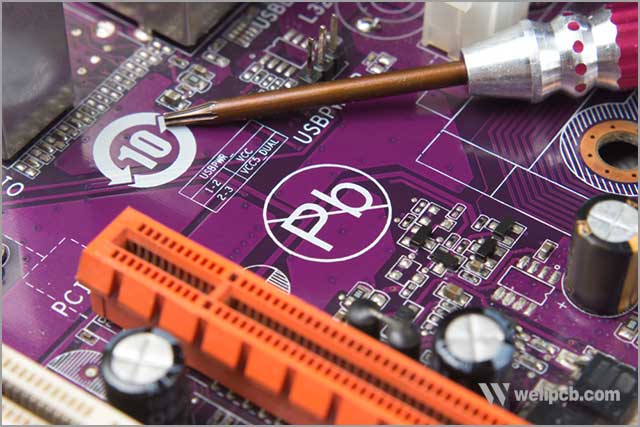
4. Separate lead-free and lead-free components
When selecting a PCB assembly, undefined lead-free parts must be separated from unclear parts to ensure a lead-free arrangement. If not specified, it is important to mark all ingredients as lead-free.

5. Assign virtual parts footprint
The virtual part contains ground and power signals. We need to consider these virtual parts during the PCB assembly schematic construction process. In the process of designing PCB components, we cannot question the importance of virtual parts.
When you keep in sync with the created bill of materials (BOM) by providing a virtual element list, you can better understand the virtual parts of the PCB assembly.
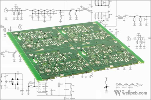
6. Make sure you have complete BOM data
Note the bill of materials data. The BOM data must be complete, and information can be obtained based on the BOM table report.
7. Sort by reference number
The reference mark (RD) is part of the BOM, which specifies the usage of each PCB component and how to find it.

8. Check the spare door
To ensure the effective operation of the entire PCB system, you must check all other obstacles. Another door is essential because you want to connect the input to the signal to act as a part that does not float.
9. We need padding
The through holes in the pads have holes to help with the PCB assembly and ensure the perfect connection between different components.
The primary function of PCB Via is to ensure that power is available between all connections in the PCB. They are essential to prevent any invasion that may cause severe damage.
10. One-touch connection
The composition of the PCB assembly must follow the one-to-one connection rules to be properly aligned during the assembly process.
11. Consider component packaging options
You should choose packaging for PCB components to complement your aesthetic design and attract customers.
Choosing a component package that can add a bit of perfection to your design will fully demonstrate your proficiency as a PCB designer.
12. The pad design matches the lead settings on the component
You need to use carefully designed pad design patterns to match the lead settings on each PCB assembly. It will automatically provide a structure for each PCB component, providing space for placing other attributes required to complete the PCB setup.
13. Address your component delivery
It has nothing to do with the design part, but this is another technique for manufacturing PCBs with perfectly shaped components. This focuses on the delivery of components. PCB components should be delivered in batches to ensure that all kits are adequately organized according to the BOM.

14. PCB on the upper and lower sides
You must consider the houses owned by the PCB. It involves paying attention to the height of the PCB (both top and bottom) to get enough PCB at the end.

Summary
The above is crucial for all PCB designers. They must remember to use incredible components to obtain the required PCB. Following these tips will provide you with a beautiful PCB, and you will also get a PCB that can meet your needs or customer needs.
Regarding the choice of PCB components, I believe you have a lot of knowledge. If you want more information, you can contact WellPCB; we can help you solve the problem and provide quality service. What are you waiting for? Please contact us!
Cloom and WellPCB are brother companies, Its covers include the value-added business of Wire harness production, assembling, custom design, and most efficient delivery route.