Start making your PCBs! Online PCB SMT Service by JLCPCB Review
Introduction to PCB SMT Service
Printed circuit boards, also known as PCBs, are frequently utilized during the manufacturing process of electronic devices. The printed circuit board (PCB) is made up of a huge variety of components, each of which may be either passive or active, and the traces on the board are used to connect the components from one side to the other. Because there are so many electronic components available in small sizes specifically for this purpose, developing large circuits on small printed circuit boards is a very simple and straightforward process. In order to have a better understanding of the benefits of utilizing PCBs, let’s take a look at some of the advantages of doing so.
What is PCB?
PCB is an abbreviation for “printed circuit board.” The board you see here is an essential component of all contemporary electronic equipment. Printed circuit boards contain an extremely high number of both active and passive components that are necessary.
DIY Projects and PCBs
Do-it-yourself projects are ones that can be completed in a short amount of time and with few resources. People have a strong preference for making relatively simple items like toys, mobiles, and the like at their place of employment or at home. Projects involving do-it-yourself electronics are extremely common among makers, hobbyists, and students. The design process for these projects takes less time, but it requires a lot of careful attention to detail.
Breadboards do not compare favorably to printed circuit boards (PCBs), and there are many reasons for this. In comparison to breadboard circuits, they offer a number of benefits, the most important of which are their more affordable price, higher level of reliability, and more compact size. Because of these features, it is simple to employ them in a wide variety of applications that make extensive use of electronic components or devices.
Why is Surface Mount Preferred?
The method of assembling printed circuit boards known as surface mount technology involves attaching the various components to the top layer of the board itself. In surface-mount technology (SMT), rather than the more conventional method of inserting components through holes and then soldering them on the opposite side of the board, the leads of the components are soldered on the same side of the board as the component itself.
Reduced costs, improved repeatability thanks to a higher level of automation, increased efficiency in the use of PCB space, and the ability to build complex circuits on small PCBs are some of the benefits of surface-mount technology (SMT). SMT was developed to cut down on the costs of manufacturing, as well as to make better use of the available space on PCBs.
Surface mount technology made it possible to build highly complex electronic circuits into ever-smaller assemblies while maintaining good repeatability thanks to an increased level of automation. This was made possible as a direct result of the introduction of surface mount technology.
JLCPCB’s SMT Service
Components that are designed specifically for use with surface mount technology are referred to as surface mount device, or SMD for short. That indicates that they have been constructed with the sole purpose of being soldered on top of the PCB. The market is stocked with a very large number of different SMDs to choose from. When it comes to JLCPCB Assembly Service, the surface-mount devices (SMDs) come from LCSC, which is the leading electronic component supplier in China.
JLCPCB can develop PCBs of various complexity. They develop Simple and cheap PCBs with Single layer boards for hobbyists and enthusiasts as well as complex multi-layer boards for high-standard industrial applications. JLC works with large product manufacturers and maybe the PCB of devices you are using such as laptop or mobile phones were made at this factory.
JLCPCB SMT Service Review
Quick and Easy Online Ordering
Pleasant online order form, straightforward Gerber file upload, trouble-free use of PayPal, and the ability to monitor the fulfillment of my order online. In addition, gerbers can be checked online (the site provides information on sizes and the minimum distances between paths), and after the file is uploaded, an online preview will be accessible (bitmaps can be saved).
How to Order?
Go to JLCPCBs website and Click on “Quote Now” and upload your Gerber File. Once the Gerber file is uploaded, it will show you a preview of your circuit board. Make sure this is the PCB Layout of the board you want. Below the PCB preview, you will see so many options such as PCB Quantity, Texture, Thickness, Color etc. Choose all that are necessary for you.

Click on “Assemble your PCB boards”. Now, you will have to upload the BOM and CPL file that we downloaded earlier. Select all the components you want JLCPCB to assemble in your PCB.

Simply click on the confirm box to select the components. In this page, you can review your order. You can check the layout, see all the components and if there is any problem, you can click on “Go Back” to edit your order.
Once everything is done, click on “Save To Cart”. In the next page, you can choose a shipping and payment option and Check Out Securely. You can either use Paypal or Credit/Debit Card to pay.
The PCB will be manufactured and shi
SMT PCB Quality
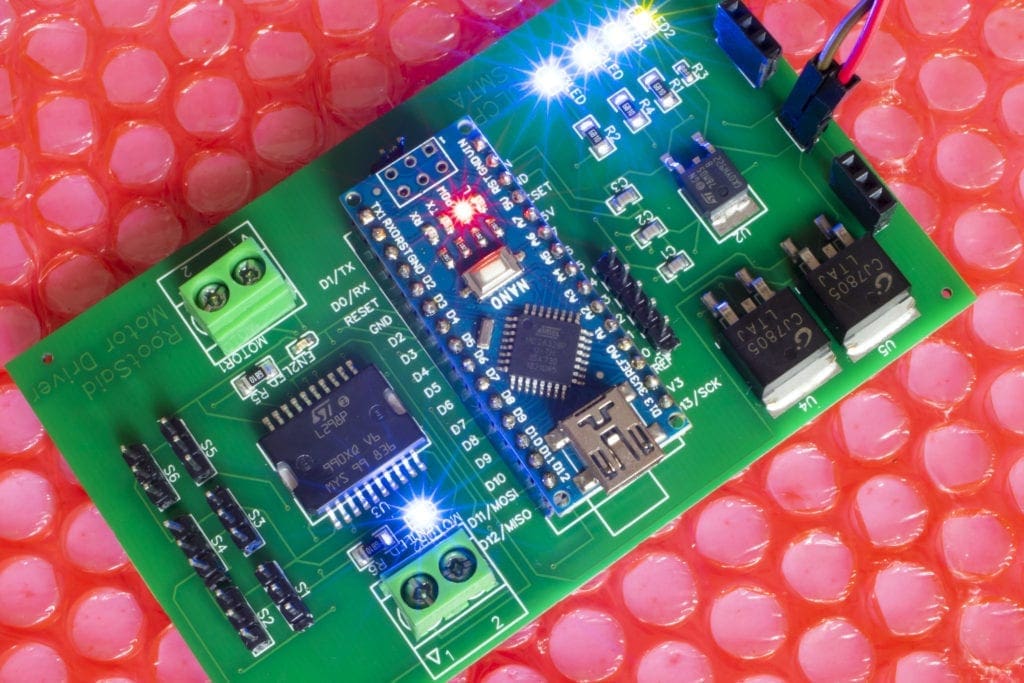
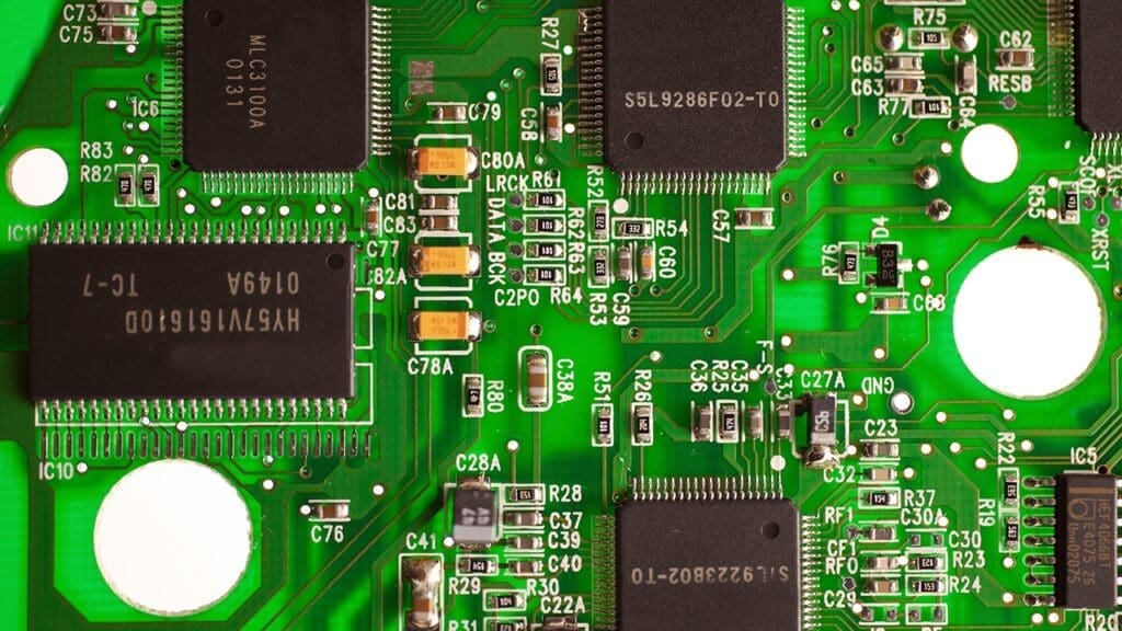
When it comes to quality, the PCBs that we get are of an astoundingly high standard. There is a seamless overlap between the patch and the silkscreen. The screen is organized and can be seen very well. Because of these shiny shoulder pads on both sides, soldering the components is a quick and simple process. Before sending out any PCBs, JLCPCB performs quality assurance checks on each one to ensure that they have a premium finish and are free of errors.
In both my hobby and professional life, I’ve found JLCPCB to be an excellent choice for the fabrication of small and large circuit boards. Always speedy and of high quality.
They have a fantastic user interface that will make it easy for even inexperienced people to begin PCB building right away without any problems.
Due to the presence of these pads, the process of soldering on these types of PCBs is made much simpler and more enjoyable for me personally. The solder takes on the shape of a cone and is soldered evenly on all sides as it rotates around the cone. The PCB looks like this once the soldering process is complete.
PCBs with low Electronic Noise
A disturbance that is caused to the desired signal while it is being transmitted or received is referred to as electronic noise. When unwanted signals are produced anywhere along the circuit, whether by the source itself or any of the other components, electronic noise is produced.
JLCPCB’s printed circuit boards have several benefits, one of which is the reduction of electronic noises in circuits, which leads to an increase in the circuits’ level of dependability. Because of this, the performance and quality of devices that contain PCBs are improved even further. This is because there are no unnecessary fluctuations or surges to disrupt the signals that are being sent through the circuit.
PCBs have a relatively low level of electronic noise, which helps us eliminate disturbances that aren’t wanted in our signals. This ensures that we are able to receive signals that are undistorted and free of background noise.
Made a mistake? No worries!
On one occasion, I made an error while drawing the layout, but I didn’t even notice it until after I had paid the full amount of money. I was able to cancel the order at any time, even after the payment was processed, and they promptly refunded the full amount to my account and explained what had gone wrong. I made the necessary adjustments, and everything turned out fine.
They do provide excellent and user-friendly customer service representatives who are there to assist you through each and every step.
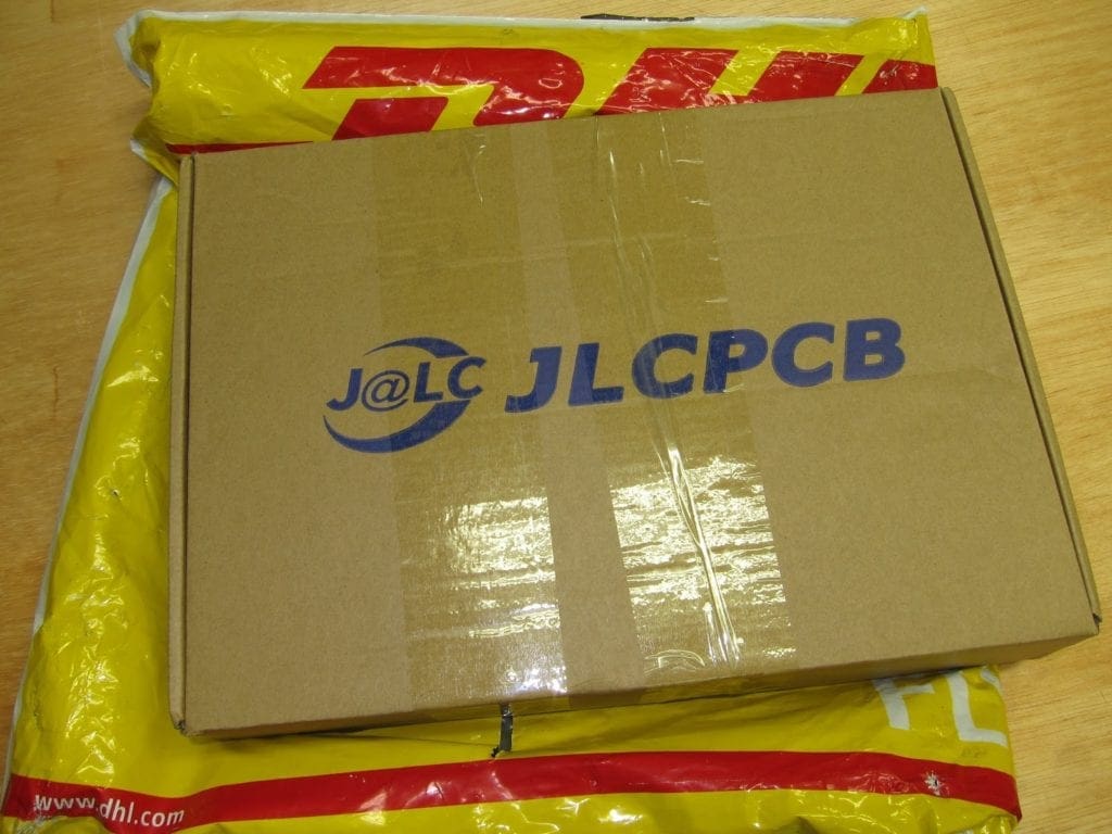
Packaging and Delivery
They do take complete responsibility for our PCBs. You will discover, once you have opened the box, that the envelope contains a cushioned wrap inside of it. In addition, a plastic wrap completely encases the printed circuit board. This guarantees that our PCBs will not sustain any kind of physical damage while they are being transported.
Along with the printed circuit board, they also send us free bonuses, such as this pen. At other times, it might be a pen; other times, it might be magnifying sheets, cello tapes, or something similar.
JLCPCB is very professional in that it provides you with the appropriate online tools to make your PCB design, it provides very affordable production prices, and it assisted me very well when my package went missing in the mail. They reshipped the item at no additional cost and it arrived in a few weeks!
Conclusion
The fact that I did not receive even a single complaint about the service or delivery of the PCBs was something that struck me as particularly impressive about the situation. PCBs that were free of errors and affordable became available to me for the first time. After placing my order, I typically received the printed circuit boards (PCBs) within a week. PCB was tested and verified, so there won’t be any issues with the PCB design or with the PCB itself.
The overall speed, quality, and price offered by JLC have left us with a very positive impression. The user interface that is used to place orders for PCBs is very simple and straightforward. On Friday, the boards were ordered, and by Wednesday afternoon, they had been delivered to our group where they had been waiting for them. Every single one of the ten boards that we printed turned out perfectly and was of excellent quality. There is no doubt that we will print from them once more.