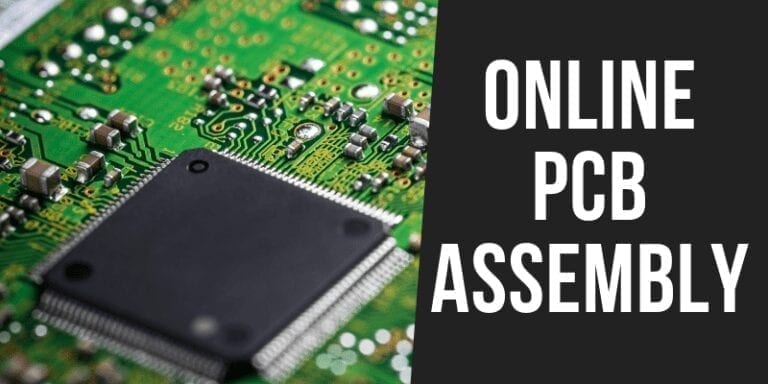
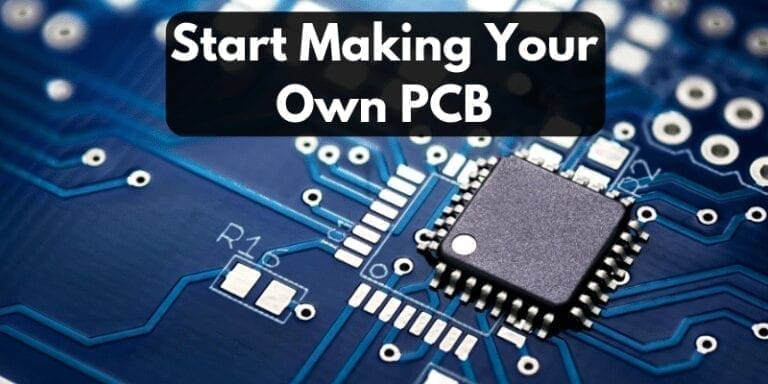
Revolutionizing PCB Fabrication: How UV Resin is Redefining the Art of Circuit Board Design
The domain of circuit board fabrication is perpetually evolving, with innovations continuously reshaping the landscape. Among the most exciting advancements in recent times is the adoption of UV resin technology. Traditionally, the process of creating circuit boards was labor-intensive, often involving manual assembly or the use of harsh chemicals that required meticulous management to avoid safety hazards. The advent of computer-aided design (CAD) software marked a significant leap forward, allowing for more precise and intricate designs through digital means.
However, the integration of UV resin into the production process represents a groundbreaking stride in the field. This technology harnesses the power of UV light to cure resin, enabling the rapid prototyping and manufacturing of circuit boards with unprecedented efficiency and accuracy. The use of UV resin offers numerous benefits, including the ability to produce highly detailed, complex patterns that would be difficult or impossible to achieve with traditional methods. Moreover, it significantly reduces production times, lowers costs, and minimizes the environmental impact by eliminating the need for harmful chemicals.
This innovative approach opens up new possibilities for customization and complexity in circuit board design, catering to the ever-growing demand for more sophisticated electronic devices. As we continue to explore the potential of UV resin in circuit board manufacturing, it is clear that this technology is not just a fleeting trend but a substantial leap toward the future of electronics fabrication, promising to redefine our capabilities in the realm of circuit board production.
The Traditional PCB Prototyping Landscape
There was a time when creating circuit boards at home was a complex, messy process, or one had to wait a long time for a professional service to send them by mail. Although making your board had its moments of pride, it was often accompanied by challenges such as messiness, delays, and minor mistakes that could set you back. Despite these challenges, these traditional methods laid the groundwork for future innovations in the field.
Enter UV Resin
UV resin is a photosensitive material that hardens under ultraviolet light, a characteristic that’s been a boon for 3D printing enthusiasts. In the context of PCB prototyping, it’s the superhero we didn’t know we needed. Instead of layering a PCB with Photoresist, exposing it through a mask, and developing it like an old film photo, we can now apply a layer of UV resin directly to the copper and expose it with pinpoint accuracy using an SLA (Stereolithography) printer.
How UV Resin Transforms PCB Prototyping
Consider the process of crafting a circuit by directly printing it onto a copper board using laser technology, eliminating the need for traditional photoresist and development steps. The precision and detail this method allows for are truly remarkable. Reflecting on an initial venture into using this technique, the goal was to produce a detailed, compact design—a task that would have presented considerable challenges with conventional approaches. Fortunately, the utilization of UV resin technology facilitated this complex task with ease.
The Role of SLA Printers
SLA printers, long recognized for their dominance in the 3D printing space, have embraced a new role in the field of PCB prototyping. This innovative approach involves utilizing them to cure UV resin on copper boards, achieving resolutions high enough to bring even the most intricate designs within the realm of home prototyping. The initial experience of substituting 3D printing resin with UV-sensitive PCB resin might seem like venturing into uncharted territory. However, this step reveals a broader trend of joining a community of pioneers who are exploring new possibilities and applications in technology.
A New Era for DIYers and Hobbyists
The implications for hobbyists, DIYers, and small-scale developers are profound. No longer constrained by the limitations of traditional etching or the cost of professional fabrication for every prototype, we can iterate designs rapidly, test concepts, and innovate at a pace that matches our imagination. This democratization of high-resolution PCB prototyping means our only limit is our creativity (and perhaps our budget for UV resin).
Challenges and Considerations
It’s not all sunshine and perfect circuits, though. Working with UV resin requires a bit of a learning curve, from applying the resin evenly to mastering the settings on your SLA printer. And, of course, safety first—resin can be messy and requires proper handling and ventilation. But, as with any worthwhile endeavor, the initial hurdles are just part of the journey.
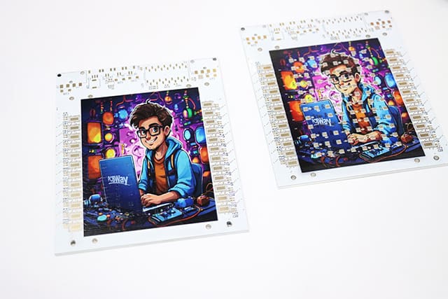
Color PCB Printing with PCBWay
In the current landscape of electronics manufacturing, the limitations of traditional PCB printing technologies have become increasingly apparent, especially when it comes to meeting the sophisticated aesthetic demands of contemporary circuit board production. In response to the evolving need for more intricate and visually appealing designs, PCBWay is excited to unveil the adoption of cutting-edge UV printing technology.
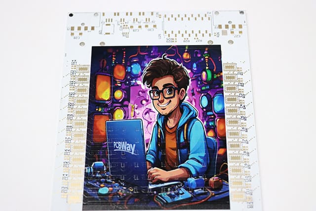
This advanced equipment employs UV-curable inks, which enable the production of high-quality, detailed images on a wide array of materials. These materials range from traditional fiberglass boards to metal and ceramic substrates, as well as flexible and rigid-flex boards. This innovation not only enhances the aesthetic appeal of the products but also expands the creative possibilities for designers, ensuring that their vision can be realized with unprecedented precision and quality.
Features
- UV-LED lamp curing is utilized for instant drying, greatly improving production efficiency.
- Utilizes UV-curable inks for durable, clear, and fade-resistant printing, improving product identification and aesthetic appeal.
- Ensures that printed information withstands SMT (Surface Mount Technology) reflow processes, maintaining integrity and legibility.
- UV printing technology supports a wide range of colors and styles, accommodating personalized customer preferences. High-precision, industrial-grade UV printers ensure exceptional quality on both flat panels and rolled materials.
- This method is environmentally friendly, emitting no volatile organic compounds (VOCs) during production, thus maintaining air quality in the workshop and promoting a safer, healthier work environment for employees.
Prerequisites for Ordering
- Maximum size for a single piece: 270*470MM
- Selection of background solder mask color required
Looking to the Future
What excites me most is thinking about where we go from here. As more enthusiasts adopt UV resin for PCB prototyping, we’re bound to see further innovations, from new types of resin designed specifically for electronics to SLA printers optimized for etching accuracy. The community around this technology is vibrant, sharing tips, tricks, and triumphs that drive us all forward.
Conclusion
Reflecting on the evolution from manual etching techniques to the advanced capabilities provided by UV resin and SLA printers underscores the rapid pace of innovation in electronics. This transition highlights the wealth of opportunities available not only to experienced electronics engineers but also to hobbyists eager to bring their latest inventions to life. The UV resin method for PCB prototyping stands out as a significant asset in the creative process.
It’s an invitation to engage, experiment, and exchange insights. Through active exploration and sharing of experiences, the community can accelerate learning and innovation. Your next endeavor could very well redefine the limits of PCB design. The electronics realm is expansive and continuously evolving. By welcoming new methodologies, reflecting on past practices, and maintaining a spirit of creativity, the journey in electronics can be both enriching and transformative.