Unveiling the Ultimate Guide: Design Your PCB Like a Pro
When it comes to modern electronics, printed circuit boards (PCBs) are the foundation of innovation. Every electronic device, from your smartphone to sophisticated medical equipment, relies on these crucial components. This guide will help you navigate the world of PCB design like a professional, covering everything from the best design software to cost-saving secrets and troubleshooting hacks. Let’s dive in and discover how you can create high-quality PCBs that will be the best choice for your electronics projects.

PCB Design Basics
What is a PCB?
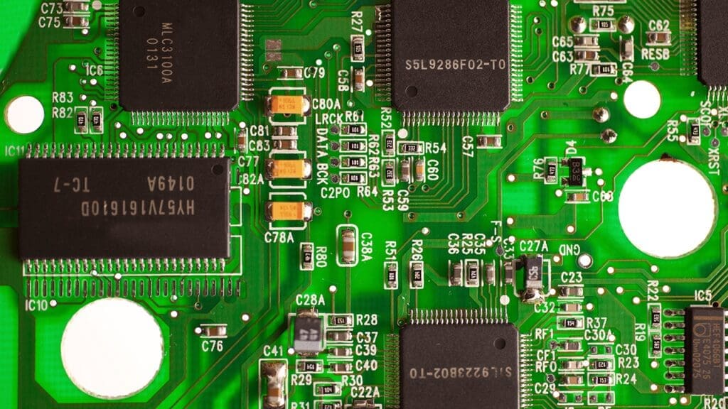
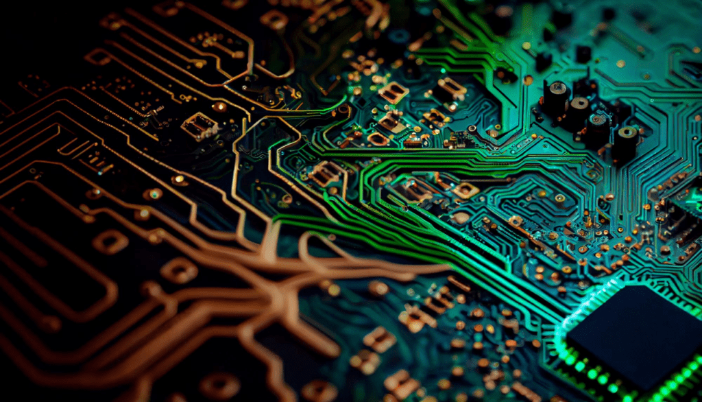
A printed circuit board (PCB) is a flat board that physically supports and connects electronic components using conductive tracks, pads, and other features etched from copper sheets laminated onto a non-conductive substrate. The importance of PCBs in electronics cannot be overstated—they provide the structure and pathways that allow electronic devices to function efficiently and reliably.
PCB Design Process
Designing a PCB involves several critical steps. First, you create a schematic diagram, which is a blueprint of your circuit showing how all components are interconnected. Next, you lay out the PCB, arranging components on the board and routing the connections. Finally, you finalize the design, ensuring it meets all manufacturing requirements and specifications. Each step requires precision and attention to detail.
Key Factors in PCB Design
When designing a PCB, several factors must be considered to ensure optimal performance and reliability. Component placement is crucial—improper placement can lead to signal interference and other issues. Signal integrity is another important aspect; ensuring that signals are transmitted without degradation is vital for the device’s performance. Additionally, power distribution and thermal management must be carefully planned to prevent overheating and ensure stable operation.

Choosing the Best PCB Design Software
Selecting the right PCB design software is a critical step in your design process. There are several popular options available, each with its strengths and weaknesses:
- Altium Designer: Known for its advanced features and robust simulation capabilities, it’s a favorite among professionals.
- Eagle: Popular among hobbyists and small businesses for its user-friendly interface and integration with Autodesk.
- KiCad: An open-source tool that offers a great balance between functionality and cost, making it ideal for beginners and small-scale projects.
- OrCAD: Preferred for its powerful features and extensive component library, suitable for complex designs.
Features to Look for in PCB Design Software
When choosing PCB design software, look for the following features:
- User-Friendly Interface: An intuitive interface makes the design process smoother and more efficient.
- Simulation Capabilities: These allow you to test your design virtually before physical production, saving time and resources.
- Component Library: A rich library of components speeds up the design process and ensures compatibility.
- Design Rules and Constraints: Tools that help you adhere to design rules and constraints ensure your design is manufacturable.
Tips for Selecting the Right Software for Your Project
Consider the complexity of your project, your budget, and specific requirements when selecting software. For beginners, tools like KiCad or Eagle are more accessible and cost-effective. Professionals working on complex projects might prefer Altium Designer or OrCAD for their advanced features and extensive capabilities.
Cost-Saving Methods in PCB Fabrication
Factors Influencing PCB Fabrication Costs
- Several factors affect the cost of PCB fabrication:
- Board Size: Larger boards require more material and are more expensive.
- Number of Layers: Multi-layer boards are costlier to manufacture.
- Material Quality: Higher-quality materials offer better performance but at a higher cost.
- Design Complexity: More complex designs take longer to produce and cost more.
- Production Volume: Larger orders typically reduce the per-unit cost.
Strategies for Minimizing Costs Without Compromising Quality
To save on costs without sacrificing quality, consider the following strategies:
- Optimize Your Design: Minimize board size and layer count where possible.
- Use Standard Components: Standard parts are cheaper and more readily available.
- Select Cost-Effective Materials: Choose materials that meet your needs without unnecessary over-specification.
- Batch Orders: Ordering in larger quantities can lead to significant savings.
Insider Tips for Optimizing Your Design to Reduce Manufacturing Expenses
Simplify your design where possible, avoiding unnecessary features that increase complexity and cost. Work closely with your manufacturer to identify cost-saving opportunities and ensure your design is optimized for their processes. This collaboration can lead to significant cost reductions and a smoother manufacturing process.
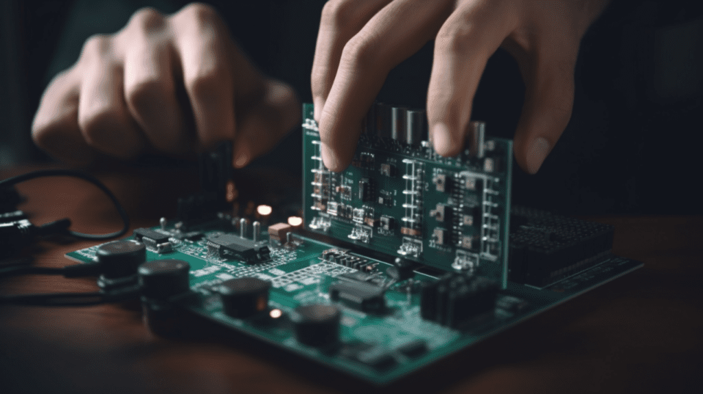
PCB Assembly Techniques
PCB Assembly Process
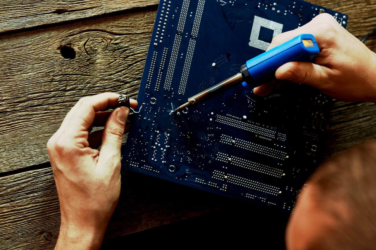
PCB assembly involves placing and soldering components onto the board. This can be done through automated processes like surface mount technology (SMT) or manually for through-hole components. The assembly process is crucial for ensuring the reliability and performance of the final product.

Best Practices for Soldering Components Onto a PCB
- Proper soldering is essential for creating reliable connections. Here are some best practices:
- Use Clean and Properly Tinned Soldering Irons: This ensures good heat transfer and clean joints.
- Choose Appropriate Solder Types: Different solders are suited for different applications.
- Maintain Correct Temperatures: Overheating can damage components, while underheating can lead to poor connections.
Advanced Assembly Techniques for Improved Reliability and Performance
Advanced techniques like reflow soldering for SMT components and wave soldering for through-hole components can enhance the reliability and performance of your PCBs. Additionally, consider using conformal coating to protect your board from environmental factors like moisture and dust.
Troubleshooting Hacks for Common PCB Issues
Identification of Common PCB Problems
Common PCB problems include solder bridges, open circuits, shorts, and component failures. These issues can arise from design flaws, manufacturing defects, or assembly errors.
Troubleshooting Process
To troubleshoot PCB issues, follow these steps:
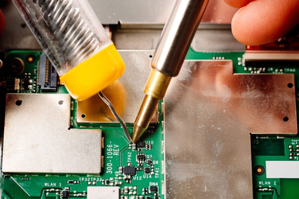
Visual Inspection: Begin by carefully examining the PCB for visible issues such as solder bridges, component misalignment, or obvious damage. A magnifying glass or microscope can help you spot small defects. Look for signs of burnt components, loose connections, or any discoloration that might indicate a problem.
Testing Connections with Multimeters: Use a multimeter to check the continuity of traces and connections. Set the multimeter to the continuity test mode and probe the points to ensure there are no open circuits. This step helps identify breaks in the circuit that are not visible to the naked eye.
Signal Testing with Oscilloscopes: For more complex issues, use an oscilloscope to analyze signal integrity. Check for proper signal levels and timings at various points in the circuit. This tool helps you visualize signal behavior and pinpoint where the signal might be getting distorted or lost.
Referencing the Schematic: Always have your schematic on hand to trace and isolate issues. Compare the physical PCB to the schematic to ensure all connections are as designed. This step is crucial for identifying discrepancies between the design and the actual implementation.
Reflow Soldering: If you find soldering issues, consider reflowing the solder joints with a hot air gun or a reflow oven. This technique can resolve cold solder joints and improve the reliability of connections.
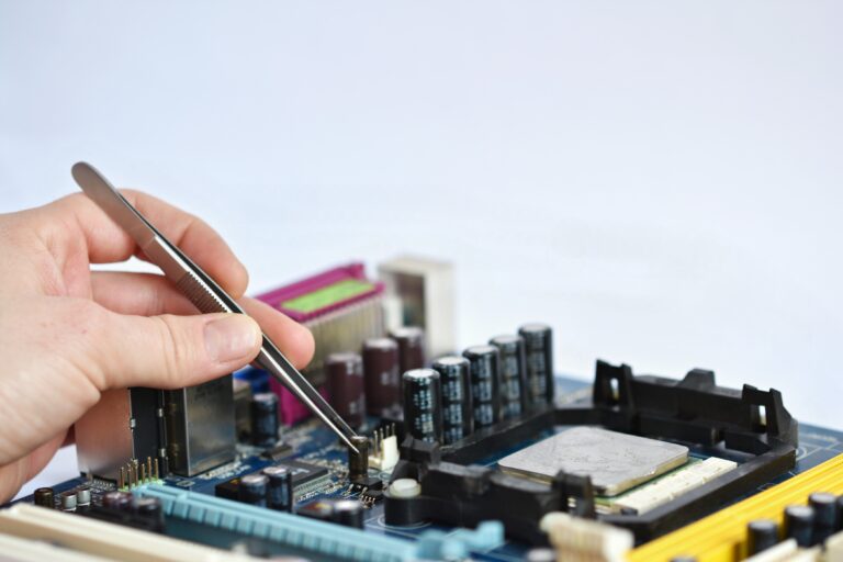
Replacing Faulty Components: If a component is found to be defective, carefully desolder it using a solder wick or desoldering pump, and replace it with a new one. Ensure the replacement is correctly oriented and securely soldered.
Documentation: Document any issues found and the steps taken to resolve them. Keeping detailed records helps in understanding recurring problems and improving future designs.
PCB Manufacturing Trends
Latest Trends in PCB Manufacturing
Like every sector it is so important to be updating continuously with the latest trends. Here are some of the most impactful trends currently shaping the PCB manufacturing industry:
Flexible PCBs: Flexible PCBs are gaining popularity due to their versatility and ability to fit into unconventional spaces. They are used in wearable technology, medical devices, and advanced consumer electronics. Their flexibility allows for innovative design solutions that were previously impossible with rigid boards.
High-Density Interconnect (HDI) Boards: HDI boards are characterized by their high wiring density per unit area, which allows for more compact and powerful electronic devices. They use finer lines and spaces, smaller vias, and higher connection pad density, making them ideal for smartphones, tablets, and other miniaturized electronics.
Advancements in Material Science: New materials are being developed that offer improved performance, such as better thermal management, higher electrical conductivity, and greater durability. Materials like polyimide, ceramic, and metal core PCBs are being increasingly used in applications that require high performance and reliability.

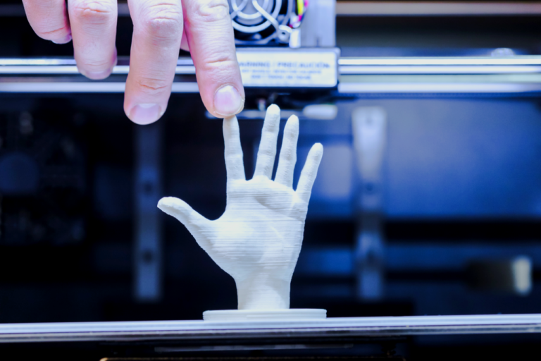
Additive Manufacturing: Also known as 3D printing, additive manufacturing is making waves in the PCB industry. This technology can achieve the development of complex PCBs more efficiently compared with traditional techniques. It also enables rapid prototyping and can significantly reduce time-to-market.
Automated Optical Inspection (AOI): AOI systems use cameras to automatically scan PCBs for defects such as soldering issues, component misalignment, and surface defects. This technology improves quality control, reduces the need for manual inspection, and helps in identifying problems early in the production process.
Solder Paste Advancements: The development of new solder pastes that offer better performance, such as improved thermal stability and reduced voiding, is enhancing the reliability of PCB assemblies. These advancements are particularly important for applications requiring high reliability, such as automotive and aerospace industries.
Impact of Trends on PCB Design and Fabrication Processes
Staying abreast of these trends enables you to create cutting-edge designs that meet market demands. Incorporating the latest technologies and methodologies into your design process can improve performance, reduce costs, and enhance the reliability of your products. For instance, using HDI technology allows for more compact and efficient designs, while flexible PCBs can open up new possibilities in wearable and portable devices. Adopting additive manufacturing can accelerate your prototyping process, allowing you to bring products to market faster.
Through-Hole and Surface Mount Technology
Through-hole technology involves inserting component leads into drilled holes on the PCB, whereas surface mount technology (SMT) places components directly onto the board’s surface. Each method has its unique advantages and applications.
Through-Hole Technology: Offers robust connections and is suitable for high-stress environments. However, it takes up more space and is generally slower to assemble. It is often used in applications requiring high reliability, such as aerospace and military electronics, and for components that need to withstand mechanical stress.
Surface Mount Technology: Allows for smaller, more compact designs and is faster to assemble. SMT components are placed directly onto the surface of the PCB and are typically used in high-density applications like smartphones, computers, and other compact electronic devices. However, SMT is less durable under mechanical stress compared to through-hole components.
Considerations for Choosing Between the Two Technologies in PCB Design
Choose the appropriate technology based on your application’s requirements. SMT is ideal for modern, compact electronics, while through-hole is better for prototypes and applications requiring high reliability and durability. Often, a combination of both technologies is used in a single design to leverage the benefits of each.
PCBWay
A passion for PCB projects leads to a variety of practical chances to investigate electronics and technology. By working on PCB projects, hobbyists can put their theoretical knowledge to use, sharpen their practical abilities, and let their creativity run wild when creating circuit layouts. If you’re an electronics hobbyist or enthusiast, PCBWay is the ideal option for you if you’re interested in creating PCB projects.
PCBWay is a leading PCB manufacturing and assembly service provider, that aligns seamlessly with the latest trends in PCB technology. In order to satisfy a variety of design requirements, the platform integrates innovative production techniques, which accommodate trends like the integration of flexible substrates and high-frequency laminates.

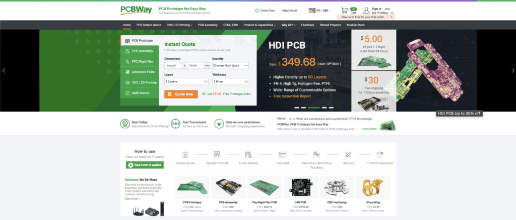
High-density components, flexible substrates, and elaborate designs can all be integrated thanks to PCBWay’s sophisticated fabrication techniques. The platform also offers consumers extensive customization choices, enabling accurate specifications catered to unique project requirements. PCBWay is the go-to option for anyone looking for dependable and cutting-edge PCB solutions because of its dedication to quality, rapid turnaround times, and user-friendly interface.
PCBWay has established itself as a reliable option for professionals, amateurs, and electronics enthusiasts looking for excellent PCB fabrication services because of its dedication to high-quality production, affordable prices, and quick turnaround times. One unique platform that encourages cooperation, innovation, and knowledge exchange among experts, hobbyists, and electronics enthusiasts is PCBWay’s Project Community. People can demonstrate their PCB creations in this dynamic community, share ideas, and get ideas from the wide variety of technologies on exhibit.
Conclusion
Here, we have included the essentials of PCB design, including choosing the right software, cost-saving strategies, assembly techniques, troubleshooting hacks, and staying updated with the latest manufacturing trends. And also explored the differences between through-hole and surface mount technology and provided detailed steps for troubleshooting common PCB issues.
With careful planning, the right tools, and a commitment to continuous improvement, you can create high-quality, reliable PCBs that meet the demands of today’s market. Keep exploring and learning, and stay tuned for more expert insights and resources on PCB design and manufacturing. By staying informed and proactive, you can continue to innovate and excel in your PCB design projects.