Methods To Find Defects In PCBs
In the field of electrical and electronic engineering, a printed circuit board is a material used to make orderly connections between various electronic components. PCBs are used to mechanically support and electrically integrate electronic parts via conductive pathways etched from copper sheets mounted on a non-conductive base.
The use of printed circuit boards (PCBs) is critical to the efficient operation of any electronic device. Nearly every electronic device has a PCB installed, and the success of such devices’ functionality is contingent on the quality of the PCBs. If the PCBs in an electric machine don’t work properly, the machine as a whole might not work. With this in mind, teams are focusing in this sector to build PCBs that are devoid of errors.
It is essential to carry out inspections at each stage of the printed circuit board (PCB) manufacturing process. This ultimately aids in finding and correcting defects in a PCB, and some of the approaches that may be used to find the defects in PCBs are discussed here.

Methods To Detect The Defects on PCB
Is it absolutely important to find the defects in the PCBs? In order for manufacturers to ensure that printed circuit boards (PCBs) function as designed, they need to check that all of the components have been appropriately built. This can be accomplished through the use of a variety of methods, ranging from fundamental human inspections to complex automated testing that make use of specialized PCB defects finding equipment. Given below are the different methods to find defects in PCBs.

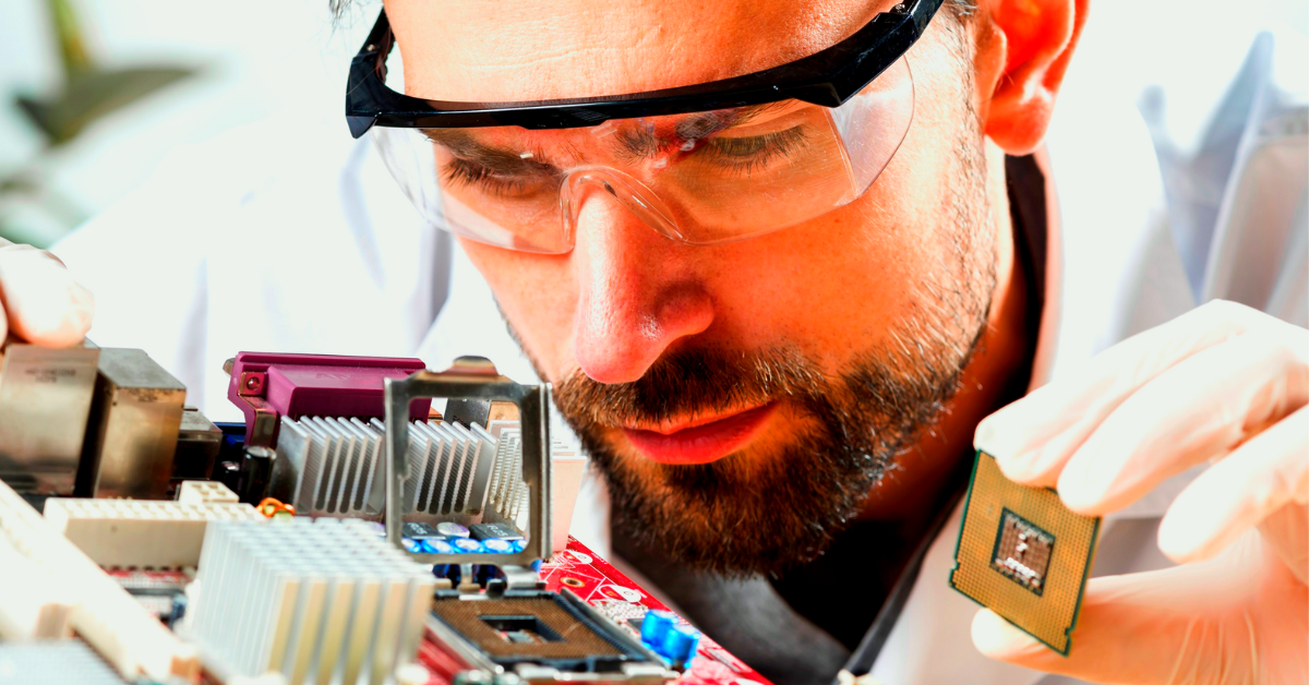
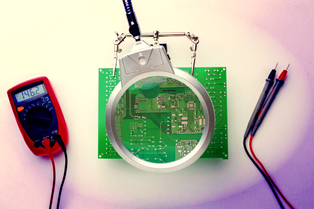
Manual Visual Inspection
Manual Visual Inspection (MVI) is the most basic method to find defects in PCB. A worker looks over the board with the naked eye or through magnifying lens to execute this type of examination. They will check the board against the design specifications to make sure all specifications were satisfied. They will also search for common defaults.
Depending on the inspection goals, you can choose specific tools for visual inspection. A prism is often used to check the reflow solder joints on a PCB. This helps find different manufacturing flaws. With prism spectroscopy, light rays that hit the PCB or PCB joints can be reflected back to figure out what’s wrong with the PCB’s design and layout. This method has limited capabilities. It does not allow you to check components that are not accessible to users.
Automatic Laser Test Measurement
Measurement from an automated laser test (ALT) is another method to find the defects in PCB. The reflectivity of various components as well as the size of solder joints and solder joint deposition may all be measured using ALT.
In an ALT system, lasers are used to scan and measure PCB assemblies. As the light bounces off the board’s parts, the system uses where the light is to figure out how high the parts are. It also measures how strong the reflected beam is to figure out how reflective the part is. The system then compare these measurements to the board’s design specs or to a board that has already been approved as correct to find any problems. An ALT system is suitable for assessing solder paste deposition quantity and position, as well as alignment, viscosity, and cleanliness. The ALT approach immediately delivers detailed information. These measurements are accurate yet susceptible to interference and shielding.
Automated Optical Inspection
A PCB inspection machine can also be used to do a visual check. This technique is referred to as automated optical inspection (AOI). PCBs are scanned using single or many video cameras during automated optical inspection. The camera saves photos of multiple elements taken from various angles and positions. These photos can then be analyzed by designers or engineers during PCB assembly to discover problems such as scratches, stains, markings, and other dimensional defects. We can also discover skewed or improper elements using this way. As a result, systems can employ various 3D AOIs to identify the height and width of PCBs, as well as the various micro components used on the PCB.
Like Manual visual examination, it can’t inspect components hidden under ball grid arrays (BGAs) and other types of packaging. It shouldn’t work well for PCBs with a lot of components, because some of them might be hidden or in the shadows.
X-Ray Inspection
After mass production, there may be problems with the inspection of parts, the soldering, the alignment of parts, etc. With X-Ray Inspection technology, X-rays are pointed at the PCB components, which absorb the X-rays to make an image. X-ray inspection helps find a number of problems in wiring assembly, solder joints, packaging for semiconductors, and other places.
For more complicated boards, X-ray inspection is the best option since it has some advantages over other inspection techniques, such as the ability to see through chip packages. Additionally, it is effective for checking PCBs that are tightly packed and enables a more thorough examination of solder joints. The technology is somewhat more recent, complicated, and can sometimes be more pricey. If you have a large number of densely packed boards containing BGAs, CSPs, and other similar packages, it might only make financial sense to invest in x-ray inspection equipment.
Conclusion
As printed circuit boards (PCBs) serve as the structural foundation for electronic systems, it is of the utmost significance to ensure that PCBs are mechanically functional at all times. What happens if we are unable to find the defects in PCBs? It will be detrimental to the overall success of your effort. It is absolutely necessary to develop methods to find the defects in PCBs in order to ensure the proper operation of electronic circuits. In this day and age of advanced technology, there are a variety of techniques that may be utilized to find the defects in our PCBs. Each approach is rapidly undergoing an update. Even in the not-too-distant future, we may anticipate the most cutting-edge and effective techniques to find defects in PCBs.