A Closer Look into the Process of PCB Manufacturing
Printed Circuit Boards (PCBs) are an essential component of many electronic devices that we use daily, from smartphones to home appliances. The manufacturing process of a PCB involves several steps, including design, fabrication, assembly, and testing. The process is crucial in ensuring that the PCBs meet the required specifications and can function optimally. PCBs can be manufactured using various methods, but the basic steps involved in the process remain the same. In this article, we will explore how a PCB is manufactured, step by step, and discuss some of the different techniques used in the industry.

PCB Manufacturing Process
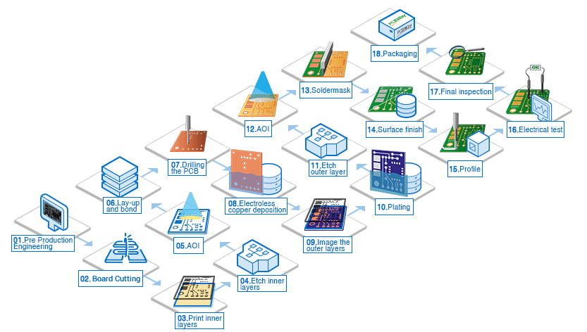
The industrial manufacturing of printed circuit boards (PCB) is going through a variety of steps aimed at converting an electronic circuit design into a hardware component. PCBs are the key part of most electronic devices to act as a base for mounting electronic components. Here are the various steps involved in the industrial manufacturing of PCBs.
Design Review and Planning
Reviewing the client’s PCB design and getting ready for production is the first step in PCB manufacturing. A CAM engineer will finish the design review and convert the design files into the manufacturing data format. The method used in this process will vary depending on the manufacturer. However, this essentially involves creating a set of step-by-step instructions for constructing the PCB. The engineer will next produce the Process Card, which includes details like the manufacturing procedures for producing PCBs, the required quantity, and the deadline. They will make sure that the resources are available based on this information, and they will create the process card outlining the production procedure.
After finishing planning, CAM Engineer will conduct a thorough data analysis and develop the tools needed to produce the PCB. The CAM Engineer will import the data into the CAM software and do basic data cleaning, such as validating file names and assignments, as well as layer alignment.
The CAM Engineer will then check the data file’s hole counts and sizes against the fabrication drawing’s specifications. Additionally, they look for any unique routing or cuts and compare plated and unplated holes. There could be several different drill and route processes, according to the demands.
Photoplotting
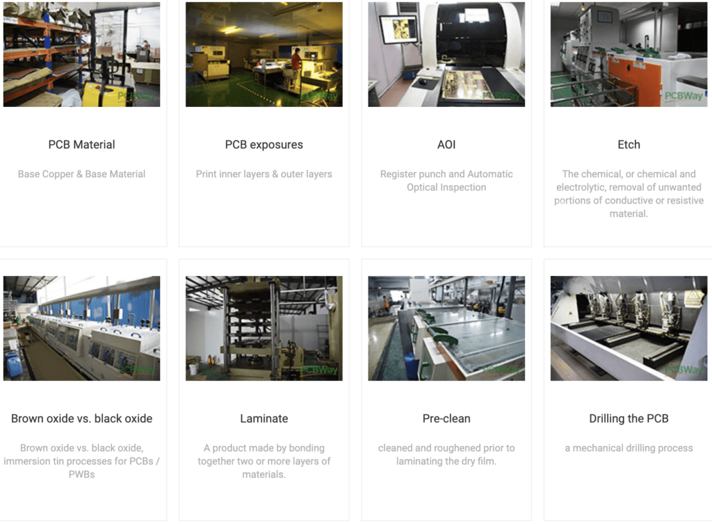
The next step in PCB manufacturing is Photoplotting. Making photolithography masks for PCBs is a technique called photoplotting. A rasterized image on film can be scanned using the electro-optical method known as photoplotting. Laser plotting is another name for it. For the purpose of fabricating PCBs, a photoplot is a film produced by a photoplotter.
For this procedure, a laser photoplotter is employed. For each distinct layer, a piece of film is created. The film is normally 18″ x 24″ in size and has a 7 mil thickness to match the most popular PCB panel size. In order to save money and improve process accuracy, specialized Laser Direct Imaging (LDI) equipment prints images directly onto dry film. The production of both internal and external layers is currently done by this process.
Developing Etch-Strip (DES)Line
The primary goal of PCB etching is to trace the circuit design on a copper plate. A coating of copper is applied to the substrate during the fabrication of PCBs. Copper layers are sometimes applied to both sides of the substrate. Etching is used to remove superfluous copper. As a result, just the necessary copper traces remain following the etching process.
There are several methods for carrying out the etching procedure. The most frequent way, however, is to employ hydrochloric acid or ferric chloride.
The copper on the PCB is covered during the stripping process by electroplated Tin or Lead. Concentrated nitric acid dissolves tin very efficiently while causing no harm to the copper circuit traces beneath the tin alloy. As a result, the PCB´s copper outline is highly visible. For the following step, the board is prepared.
Automated Optical Inspection for Multi-Layer PCBs
Multi-layer PCBs can be inspected using automated optical inspection (AOI). It is a machine-based method for testing and examining potential PCB faults. These mistakes include component placement problems, dimensional flaws, and surface errors. AOI plays a crucial role in inspecting the printed circuit board after assembly as the circuit board becomes more and more complex, making it difficult to physically check the boards.
Oxide Treatment in Multi-Layer PCBs
It is a chemical process applied to the inner layers of multi-layer PCBs to make the clad copper rougher and strengthen the binding between the laminates. This procedure aids in preventing separation between the laminate and the conductive foil as well as between any base material layer.
Lamination Process in Multi-Layer PCBs
In the process of making a PCB, the lamination procedure is crucial. Building up successive layers of a substance is referred to as lamination. Additionally, the method used to bond those layers strengthens, shields, and waterproofs a range of materials. The substrate is laminated with copper. The PCB lamination process is a crucial step in the production of circuit boards, even though the requirements differ based on the way a circuit board will be utilized.
Drilling and Electroless Copper Deposition
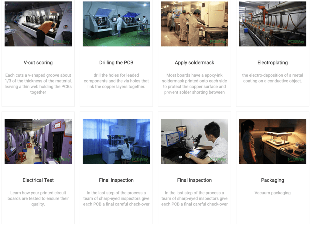
PCB drilling is the process of making cavities such as slots and holes on circuit boards. Numerous distinct hole kinds are drilled throughout the PCB drilling process. Via holes, component holes, and mechanical holes are a few of them. Because of the need for accuracy, holes are often drilled out with a manual or laser PCB drill.
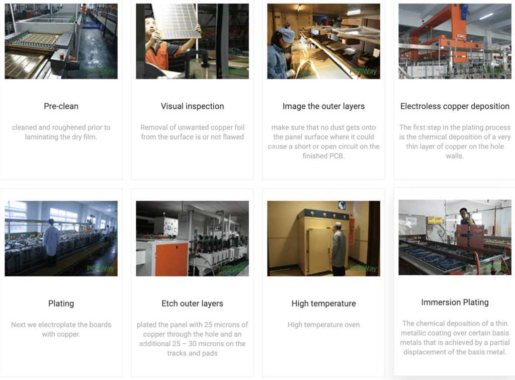
Following the drilling operation, an electroless plating technique is used to chemically deposit a thin layer of copper on every exposed portion of the panel, including the hole walls.
The primary goal is to first deposit a layer of copper on the conductive substrate before using additional electroplating techniques to increase the copper layer’s thickness to the desired level.
Making Dry Outer Layer Film
In this phase, dry film, also known as photoresist, is applied to the exposed copper panel’s outer layers using a laminator machine. After that, laser direct imaging is used to expose the dry film. The unexposed film is processed off, leaving only the exposed film. As a result, the exposed pattern and holes are ready for copper plating.
Electroplating, Stripping and Etching
Electroplating is the subsequent stage in manufacturing a PCB. The conductive surface is submerged in a copper plating solution comprising copper sulphate and sulfuric acid throughout this procedure. This causes copper to be deposited with a thickness of around 1 mil onto the conductive surface of the board when current is applied to it. After that, the plate is taken out and submerged in a tin-plating solution to act as an etch barrier.
Following the completion of plating, the dry film is taken off, and the exposed copper that is not covered by tin is etched away, keeping just the plate’s traces and other patterns. After chemically removing the leftover tin, only copper is left at specific locations.
Solder Mask, Silkscreen and Surface Finish
UV exposure will be used to apply a solder mask to the printed circuit board prior to PCB assembly. The unique green color of printed circuit boards is due to this.
A thin polymer covering called a solder mask shields printed copper lines on circuit boards from oxidation. Additionally, it avoids solder bridges, which are formed when unintended connections between two wires render a printed circuit board useless.
Further board marking and component reference designators are silkscreened onto the printed circuit board after the solder mask has been placed. Baking the circuit board in an oven cures the solder mask and silkscreen ink.
On exposed metal surfaces that are not shielded by the solder mask, a surface treatment is then used. During the PCB assembly, this aids with soldering and secures the metal.
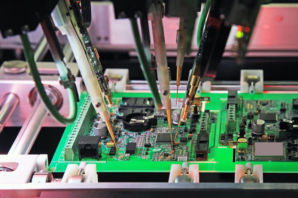
Assembly, Inspection, and Testing
Before being assembled or shipped, the finished PCBs go through a number of tests and inspections at the last stage of PCB manufacture to assure their functionality. Any shorts that may disrupt a board’s operation are sought out automatically by test equipment, and any PCBs that fail the test are eliminated.
PCBWay in PCB Manufacturing
A well-known brand in the PCB manufacturing industry, PCBWay provides comprehensive and trustworthy solutions to satisfy the various requirements of electronic enthusiasts, engineers, and organizations. As a top supplier of superior printed circuit boards, PCBWay has made a name for itself by placing a significant emphasis on quality, effectiveness, and affordability.

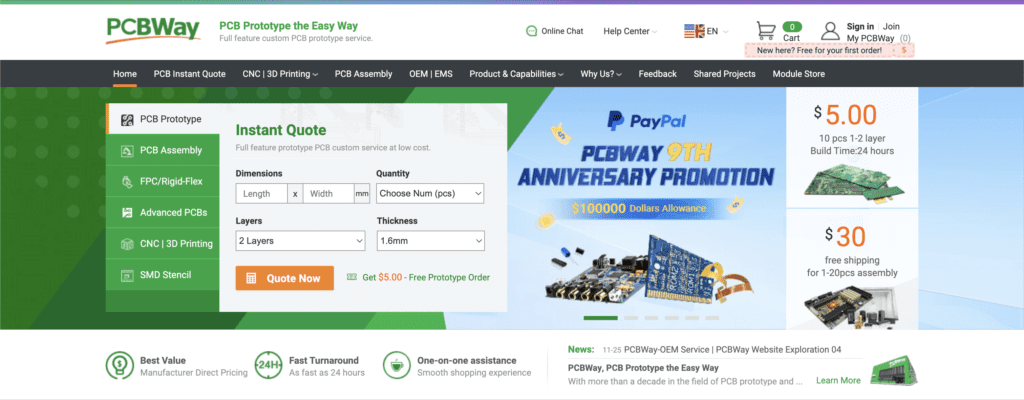
Their cutting-edge manufacturing facilities make use of cutting-edge technology and automated procedures to guarantee precise and reliable output results. PCBWay provides a wide range of manufacturing services, including assembly, small- to large-scale production, and prototype fabrication. They offer a clear and user-friendly web platform that makes it simple to place orders, track progress in real-time, and communicate effectively with their team of specialists. A trusted partner for all PCB manufacturing requirements, PCBWay has gained the trust and loyalty of customers worldwide through a dedication to customer satisfaction, short turnaround times, and low price.


Conclusion
Finally, it should be noted that PCB fabrication is essential to the design and creation of electronic gadgets. The need for superior, trustworthy, and effective printed circuit boards never goes away as technology develops at a breakneck pace. In order to ensure accuracy and consistency, the manufacturing process has undergone significant evolution, including cutting-edge technologies and automated systems. Manufacturers of PCBs, such as PCBWay, have become significant players in this market by providing comprehensive solutions to satisfy the various requirements of customers, engineers, and companies. PCB makers continue to support the expansion and innovation of the electronics sector by focusing on quality, cost, and customer happiness. This has made it possible to realize cutting-edge technical developments that are both innovative and exciting.