10 Myths About PCB Designing!
Introduction
PCBs are at the heart of every electronic device on the globe, as their purpose is to connect various components. Many of the technological devices on the market today contain printed circuit boards. And some myths about PCB designing is also there.
PCB designers must ensure that their designs are precise and will function properly in order to get a product to market on schedule and avoid manufacturing difficulties. People hear various falsehoods about PCB design, just as they do about any other area. We are dealing with the ten myths about PCB designing.
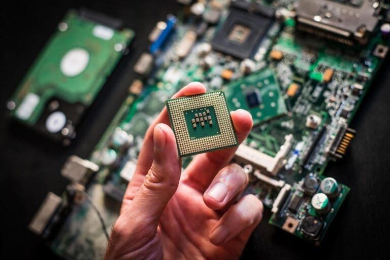
All Printed Circuit Boards are Green
One of the frequent myths about PCB designing is that all PCBs are green in color. Glass-epoxy, is the component that is utilised the most frequently in the manufacturing of printed circuit boards. However, the quality of a printed circuit board (PCB) is in no way influenced by the color of the PCB. It is possible to obtain a green printed circuit board (PCB) that is of the highest quality or a blue circuit board that is riddled with errors. When it comes to printed circuit boards (PCBs), the arrangement of the electronic components is more important than how the boards look.
The Only Complete Connection is from Pin to Pin
Most PCB designers just route the signal traces from pin to pin, and they don’t worry about timing other than making sure the traces are all the same length. But this way of making things doesn’t take into account the fact that current doesn’t just flow in one direction. It goes in a circle. And that doesn’t mean that it should just go back the way it came. The return current follows the path with the least amount of resistance or, at high speeds, the path with the least amount of inductance. As it goes back through, it charges the local parasitic capacitance. The ground plane can’t be used to get rid of unwanted signals because of this.
Trace Widths are Limited to 3 mils
It used to be true that employing trace widths less than 3,000ths of an inch resulted in issues for spans longer than very short ones. However, recent advances in semi-additive manufacturing now enable considerably smaller trace widths without creating issues.
A Region Of Zero Potential Is The Ground
One of the prevalent myths about PCB designing is that the ground has no potential. At regular DC voltages, ground has no resistance and no impedance at all frequencies. But when it concerns high speed PCB designs, “ground” is no longer feasible. There is some resistance in every metal. It can be as close to zero but the current still makes a loop, which causes inductance. When you reach such greater speeds, these seemingly small numbers become much bigger, and it becomes almost impossible to find a place with no potential at all.
The PCB Design Tools are almost Identical One to Another
To make PCBs, all you require is a platform. You might have a favourite design tool that you won’t let go of no matter how many difficulties it causes. You can’t rush or be careless when looking for a PCB design tool. Initially, you need to make a list of what you need from a design. There are many things to think about when choosing the right tool, such as the size and quality of its content library, the ease of getting help and fixing problems, how well it works with the supply chain and MCAD, and much more.
Figure out what you expect from your PCB design tool, and then look for one that can give you what you need without upsetting or changing your current processes and methods. Before you make a final decision, do your research to find out what you need, what you can fund, and what kind of return on investment you can expect.
With 90-degree Angles, Acid Traps can be an Issue
Many people think that a 90-degree angle on a printed circuit board could cause problems with the acid coating, so they try to avoid having any of those. In the past, acid traps with 90-degree angles could have caused a lot of trouble. But designers no longer have to worry about this because most PCBs aren’t etched with an alkaline solution anymore.
They are Harmful to the Health of the Environment
There is a common misconception that PCBs are harmful to the environment, although this is not totally true. People believe this because electronics can be bad for the environment, however there are initiatives to improve PCBs in general. In the near future, biodegradable PCBs will be available, and these kinds of circuits will start to get much better all around.
Your Sole Objective is to Make the Printed Circuit Board Working
When it comes to the design of printed circuit boards, you could have the impression that your only objective is to create a board that is functional, and once you’ve accomplished that, your work is finished. However, the scope of your work with printed circuit board design extends much beyond only ensuring operation at a fundamental level.
In addition to this, you need to make certain that your printed circuit board is streamlined, productive, and economical. And you definitely don’t want a printed circuit board that’s full of bugs.
Printed Circuit Board Design Software is not Platform Independent
The idea that PCB design software can only run on a single platform is another widespread misconception surrounding the design of printed circuit boards (PCBs). It’s possible that this is the case with some PCB design software, but it’s definitely not the case with all of them. Some PCB design tools can be modified to run on many platforms, such as Linux and Mac OS. These platforms include Windows.
There is no need for More Than One PCB Components Provider
You might believe that you only need one provider for components while you are searching for vendors for your newly created printed circuit board (PCB). After all, if you’ve located a place that can provide the components you require at a cost that’s acceptable to you, there’s no reason to look anywhere else.
It is critical to have a secondary source of supply on hand in the event that your primary source is interrupted for any reason. After all, you never know when your primary supplier could have an issue. Because of this, you should always have a backup source in case your original one does. In addition, a delay in the delivery of supplies may put your efforts in threat.
Conclusion
As an engineer, it is essential to remember that you cannot believe everything that you hear. It’s possible that some of these misconceptions imprinted in your head for many years. But look at them once more in a different perspective this time. In the context of your design, do they really make sense? Are these regulations now defunct as a result of recent advances in technology? Change your strategy and look for fresh approaches to the challenges you’re facing. You can contribute to the debunking of further such PCB design misconceptions if you put in the time and effort.