PCB Manufacturing Process Step By Step | JLC PCB Fabrication
PCB Manufacturing
Circuit boards are there in every piece of an electronic device in our lives. From mobile phones to satellites that orbit around the earth, these boards with silver lines play a major part in today’s world. But how are they made? What are the various PCB Manufacturing Steps? In this post, we are gonna find out what these PCB-making processes are. We will be taking a look at what is going on under the roof of one of the world’s best high-quality online PCB manufacturers around the world – JLCPCB.
PCB Manufacturing Company – JLCPCB
JLCPCB is one of the best Online PCB manufacturing companies from where you can order PCBs online without any hassle. The company works 24 hours a day, 7 days a week nonstop. With their high-tech machinery and automated workstream, they can manufacture huge quantities of high-class PCBs within hours.

JLC PCB can develop PCBs of various complexity. They develop Simple and cheap PCBs with Single layer board for hobbyists and enthusiasts as well as complex multi layer board for high standard industrial applications. JLC works with large product manufacturers and may be the PCB of devices you are using such as laptop or mobile phones were made at this factory.
PCB Manufacturing Process
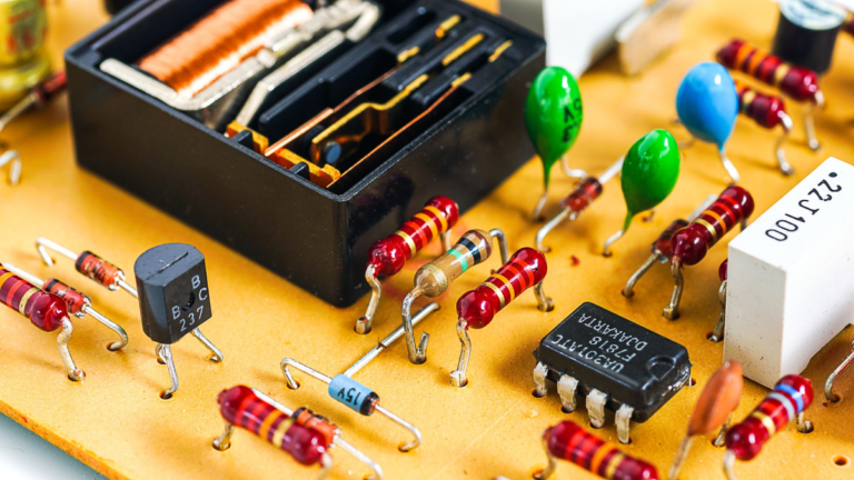
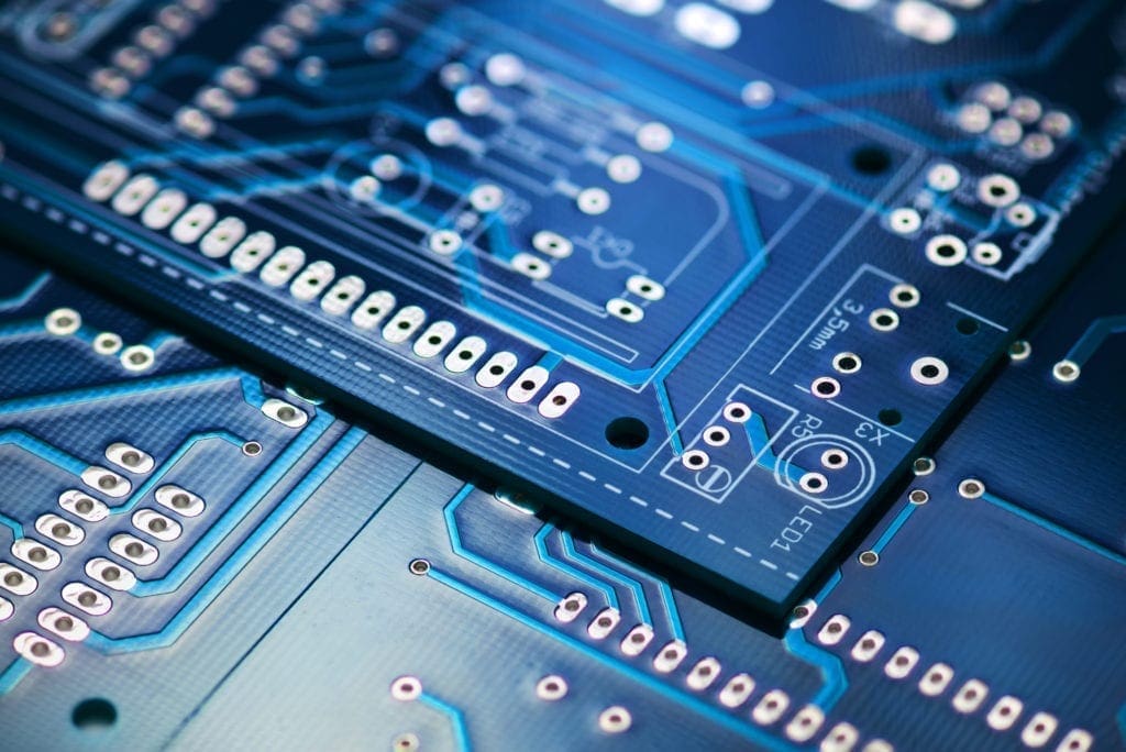
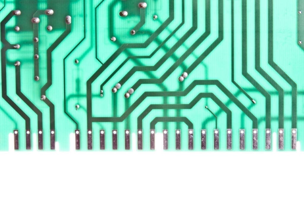
PCBs are basically a bunch of tiny copper wires sandwiched in between multiple layers of fiberglass. These tiny wires connect all the components to each other in an organized and repeatable way making a neat and tidy electronic circuit board. Here we will take a look at the PCB Manufacturing Process.
Industrial PCB Manufacturing Steps
JLCPCB is a PCB manufacturing company with a full production cycle. Which means they start from “A” and finishes with “Z” of PCB manufacturing process. From raw materials to finished products, everything is done right under the roof.
In this post, we will go through the basic of sophisticated and complex processes that JLCPCB factories take to make high quality PCBs for their customers.

Step 1 – Cutting
Raw materials like copper cladded boards are first cleaned and cut to the desired size. After cutting them into pieces, they are then moved to the next machine for processing the edges.
Step 2 – Drilling

Next job is to drill the PCB. Yes. Here, the PCBs are first drilled before processing further. There are dozens of precisely automated machines that will will drill holes in the board. These machines can also change the drill bit depending upon the diameter of the hole that is there in the PCB Layout.
After Drilling, these boards are then cleaned thoroughly using brushes
Step 3 – Deposition
In this stage of Industrial PCB Manufacturing, another layer of Copper is deposited over the boards. This is the stage where primary metallization of the holes is formed which is crucial in the creation of double sided or multilayered PCB. Again these boards are washed and cleaned.
Step 4 – Photoresist
In this stage, a thick layer of photoresist is coated over the board. After that, photomask, which contains the layout is placed over the board. Photomasks are transparent sheets where the PCB layout is printed. Once the alignment is checked, it is exposed to UV light.
Step 5 – Exposure

Here, the boards are exposed to UV light. When these boars are exposed to UV Light, the photoresist gets polymerized in the areas that are not protected by photomask. After this, the extra photoresist that remains in the PCB gets washed Off.
Step 6 – Baking
After cleaning, these boards are then baked in ovens which will increase the mechanical strength of the photoresist.
After this, a thin layer of tin – lead alloy is chemically deposited on previous copper layer increasing the reliability of all the holes. They are also deposited on copper tracks from where the photoresist was removed earlier. These are the only things that remains in the final board. Everything else will be removed during the etching process.
After so many chemical processes, the remaining photoresist is completely removed.
Step 7 – Etching
PCB etching is the process of chemical removal of unprotected areas of copper. Here the boards are transported through conveyor and jets of etching solutions are used to etch away the exposed copper. After etching, the Lead coating is removed using a similar chemical manner.
Step 8 – Quality Control

There will be some traces unwanted lead or copper left on the board. All this will be rectified at the Quality Control Center. In PCB Quality Control Center, all boards will be thoroughly checked using powerful scanning systems with optical sensors.
If any defects or errors are found, errors will be corrected automatically or manually under microscopic tests. If over defective boards are found, they are completely rejected and new boards are made with better quality.
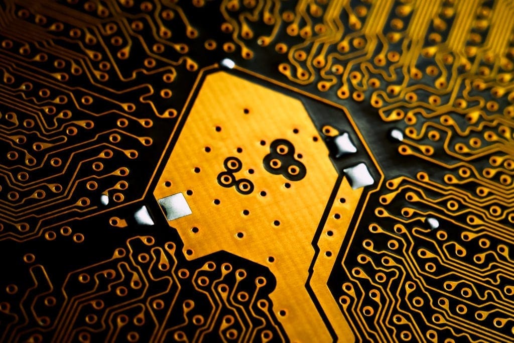
Step 9 – Masking
Masking is done over the board to protect the copper from corrosion or other harmful activities. Masking gives the board an industrial appearance. Masking can be done in any color. Usually done in green, the company offers a wide variety of colors such as blue, red, black to name a few.
Step 10 – Silk Screen Printing
This is similar to applying solder mask. This is where they add symbols such as components, logos or texts are added to the board. Again these boards are cleaned, heated and cooled to obtain high quality PCBs.

Step 11 – Surface Treatment
During this stage, bare surface of copper (where we solder the components) is coated with gold or tin plated. This will protect the copper from corrosion for decades.
Step 12 – Cutting
All the above mentioned processes are done on huge sheets. So one piece of sheet can have upto 10 identical boards. A huge number of machines are used in PCB Cutting Process.
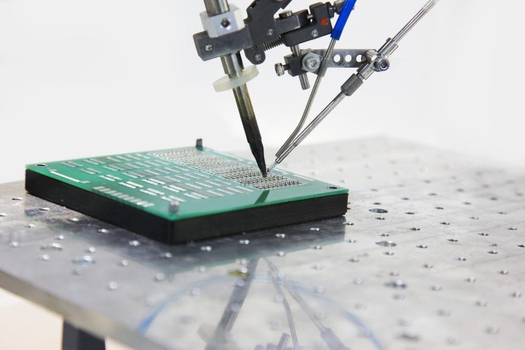
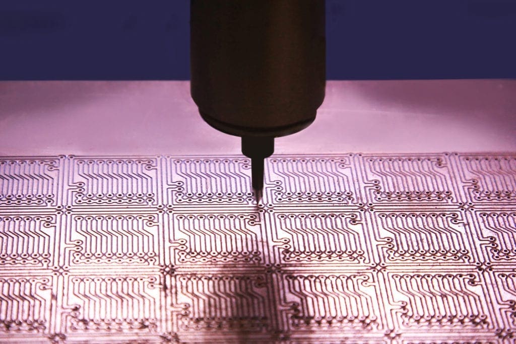
Step 13 – Testing PCBs
Here, automated machines are used to test the connections of the board one by one. They test each and every nodes using probes at incredible speed. They check all the connections and cross check it with the original Gerber File.
After this, the boards are neatly cleaned, packed and sent to customers.
[RICH_REVIEWS_FORM]
[RICH_REVIEWS_SNIPPET stars_only=”true”]
New to Robotics?
We have a beginners guide on “Getting Started with Robotics” which will give you a kick start in this field. Check out our free video tutorial below for a brief introduction.