Altium Designer PCB Tutorial: Design Arduino Board Step-by-Step [2026 Beginner Guide]
Complete Altium Designer tutorial for beginners. Learn to create schematics, place components, route PCBs, and modify board shapes. Includes free student license info + DIY Arduino project.
Altium Tutorial Introduction
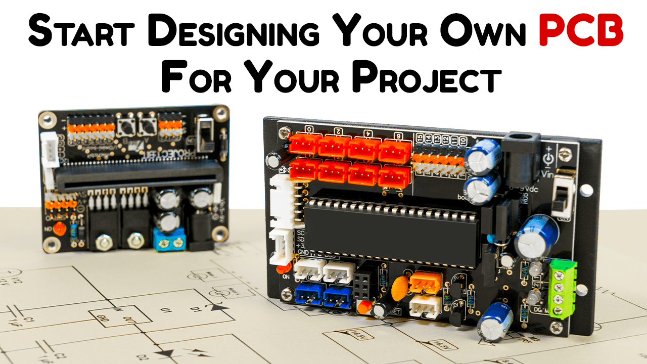
We’re glad to see you guys back! Throughout this tutorial, I’ll show you how to quickly and easily design PCBs for your DIY projects using Altium. We’ve done a lot of interesting things in the last few projects, haven’t we? We worked on a slew of Arduino-based projects, including robots, Halloween decorations, and even our own Arduino board. We used Altium to design the circuit and the PCB layout.
Many of our subscribers tried the free trial, and the results were nothing short of spectacular. In some cases, they asked me to write a tutorial on how to design a PCB layout using Altium. In fact, that’s exactly what we’ll be doing now.
In today’s Altium Tutorial, I’ll show you exactly how to use Altium to design PCBs for your hobby projects step-by-step. You should be able to design and build your own PCBs for your project if you follow all of the instructions in this post! Let’s get started with Altium Tutorial!
Altium Tutorial Step 1 – Download Altium Designer
Altium is a professional-grade PCB designer that handles everything from simple hobby project boards to complex, multi-layered industrial PCBs. And honestly, once you get the hang of it, it’s surprisingly easy to use. If you’re a DIY electronics enthusiast, this is probably the most powerful tool you can add to your workflow right now.
Altium is an amazing PCB designer with so many user-friendly tools and features like centralized cloud storage and online collaboration. You can design and create your own PCBs for your hobby projects or share your ideas across your network.

So the first step is to download and install the free trial version. Now here’s the part most beginners get confused about — if you’re a student, you can get a free full Altium Designer license through the Altium Education program. This isn’t a one-time 6-month deal. The license is renewable every 6 months as long as you’re still enrolled in an academic institution. You’ll need a .edu email address or some form of academic verification to apply. So as long as you’re a student, you essentially have free access — just remember to renew it every 6 months before it expires.
Go ahead, download and install it. Once that’s done, just open the software and we’ll get started.
If you’re still evaluating whether Altium is the right tool for your project, check out our PCB design tools comparison and our Altium vs Siemens PADS comparison before committing.
Start a New Project in Altium Designer
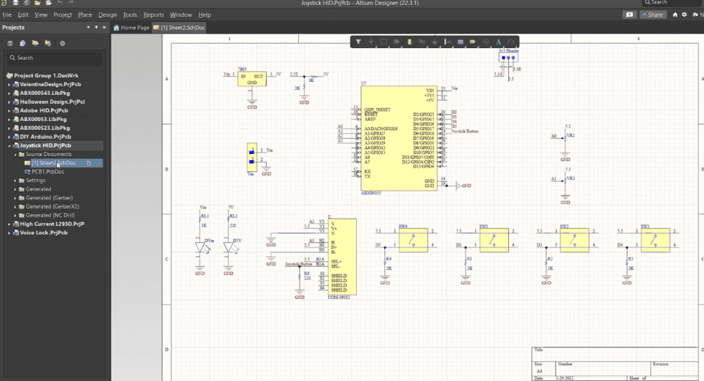
Simply open it once you open it you should see a screen like this. Here if you take a closer look you can see two windows. On the left side window, you should see all the projects and all the files in that project on the right side window you should be able to see all the files that are currently open in different tabs.

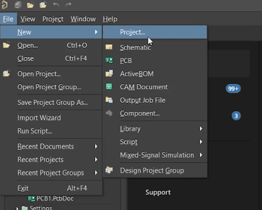
Now let’s create a project. For this video, we will be designing our own custom-made Arduino board. So, first go to files, new, and project.

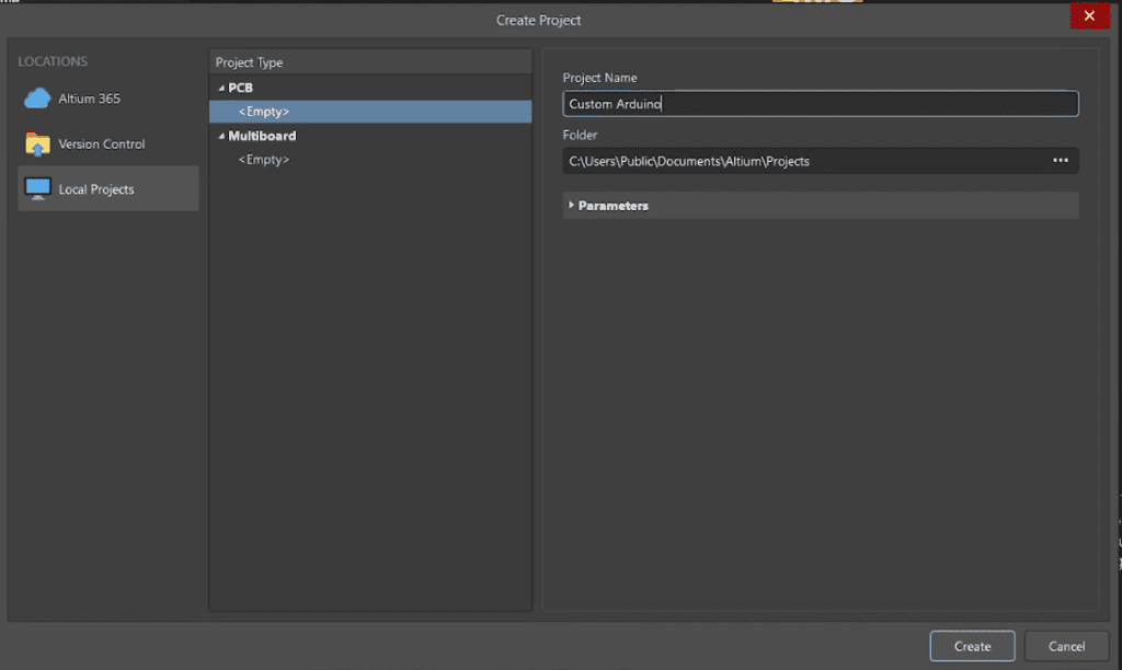
Now let’s give our project a name. Let’s name it DIY Arduino and click on create.

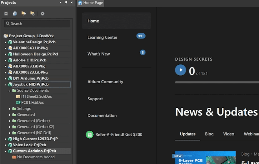
Here on the left side, you should see our new project and if you expand it, you should be able to see all the files that are used by the project. As of now, there are no files associated with this project. That’s why it’s showing empty.

Creating Files for Schematics and PCB Designing
For this project, we will need to create two files one for drawing the schematics and the other for designing the PCB layout. To create a new file simply right-click on the project add new to the project and click on schematics.

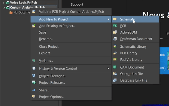
And here we go. This is where we’ll be drawing the schematics or the circuit.
Now we will have to create one more file where we’ll be designing the PCB layout for this PCB. To do that again, right-click on the project add new to the project and click on PCB and here you can see another file has been created. Both these files are opened and are right on top. You can switch between the tabs by simply clicking on them.

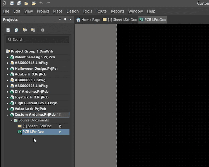
First, we’ll start by drawing the circuit. For that go to the schematics file.
Finding out the Right Components using Octopart
Now before you start adding the components to your circuit and design the final PCB, it’s always a good idea to have a good knowledge of the components such as specifications, availability as well as price. For that, I would recommend this site called Octopart. Octopart is an amazing electronic component search engine.

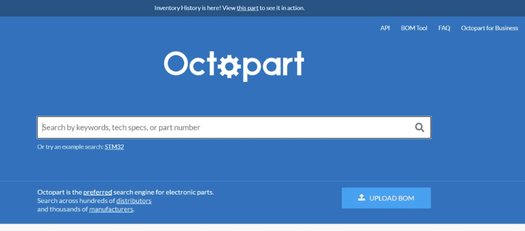
You can use octopart to get details such as distributor, pricing, and availability. You can also use octopart to find components that meet your requirement. You can even purchase the component by clicking the link here itself!

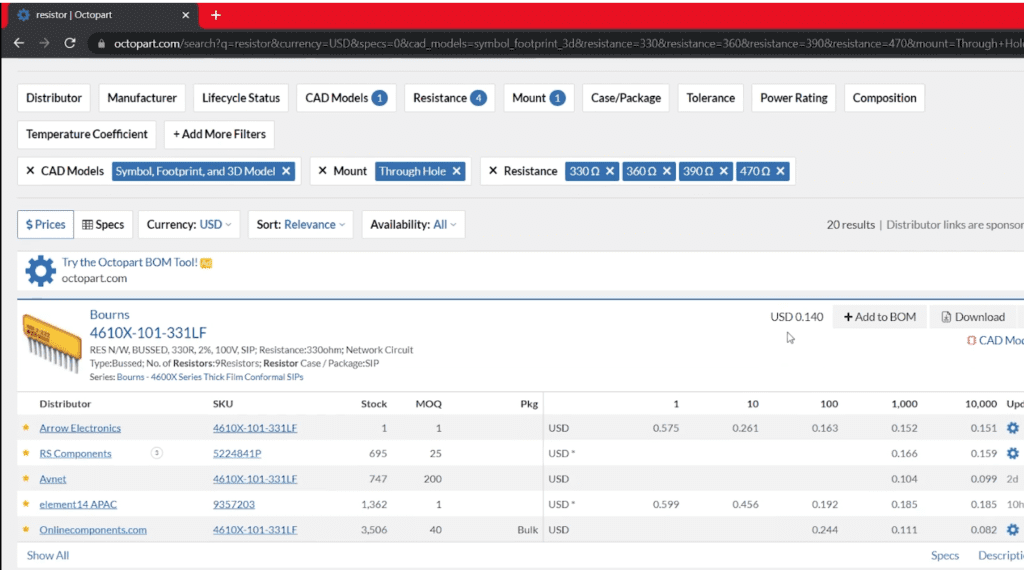
It’s A free solution for most of our problems and you will get everything in one place! This Is also gonna be really useful for you guys. Make sure you check it out! Now we will start adding components.
Altium Tutorial Step 2 – Drawing the Circuit
Finding the Right Components using Altium Components Library
In order to make our Arduino board, we will need a microcontroller which in this case is Atmega328 but the microcontroller can’t operate without the bare essentials. In order for it to function, it will need a minimal amount of component setup. Let’s look at the bare minimum configuration.
To set up a bare minimal circuit, we will need an Atmega328, an input voltage of 5V, a 16 MHz crystal oscillator, an LED, a resistor, and 2 capacitors.
On the toolbar right here can you see a yellow button? It’s called the place part.

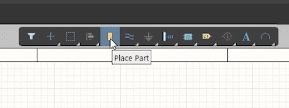
When you click on that, a component window will pop up, and there you can search for whichever components you want.

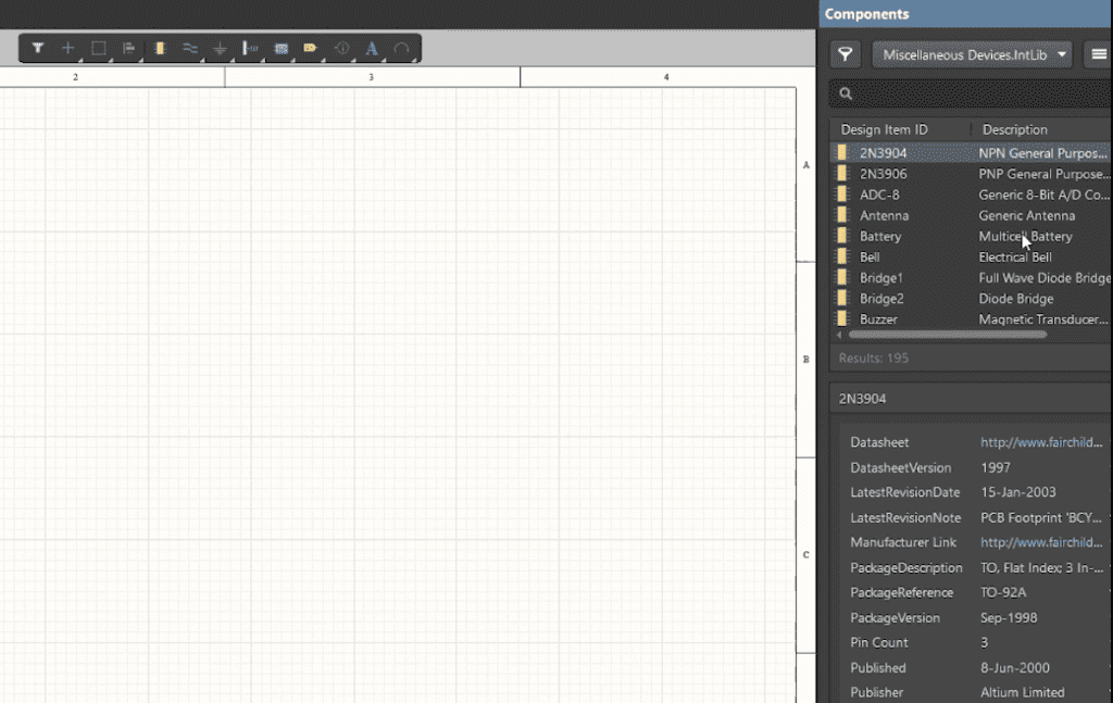
. One thing you should keep in mind while selecting a component is when you select a component, you should make sure that there is a proper footprint available. For that component footprint, details will be shown below the component details.

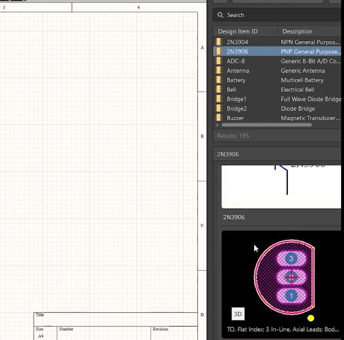
Placing Components from Library to the Schematic File
Now let’s place our first component led. Simply search for LEDs and below that you should see a list of all LEDs available. Here some of them are SMD components some of them are normal LEDs. Check the details and footprint and make sure you select the right one alright. Let’s add it to the circuit. To add the component simply right-click on the component and click on place. The cursor will change. You can click anywhere on the schematics. Let’s place it right here.

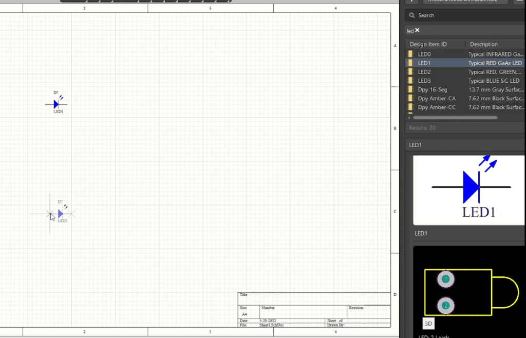
And here we go. Now let’s follow the same steps to add the remaining components. If you want to rotate the component simply press on the spacebar. It will rotate 90 degrees.
Component Out of Library? Search for Additional Manufacturers’ Component
And now let’s add an Atmega328 IC. There are so many different versions of Atmega328 ICs available and some are preloaded with Arduino Bootloaders. You can easily find the right one using Octopart!
Sometimes, the part you are looking for might not be in this library.

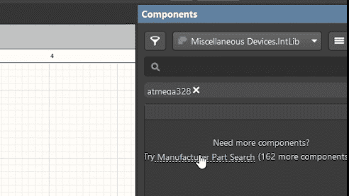
In that case, we can browse additional components by clicking on the manufacturer part list.

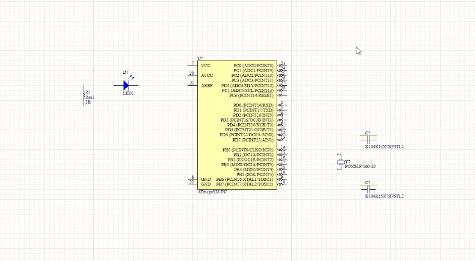
Alright! Now We have added all the basic components. Now, let’s connect them together and draw the circuit!
Connecting the Components in Altium Schematic File
Now we have all the components added to the canvas of the schematics file. Next, we need to connect them together and draw the circuit. There are mainly 2 ways we can do that.
Connecting Components wsing Wiretool
For that click on the wire tool and you can see the cursor has changed right simply click on any terminal of a component.

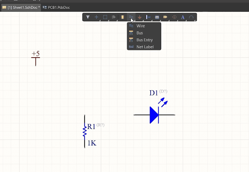
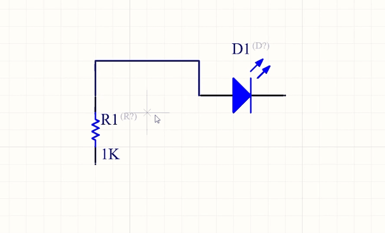
Let’s connect the LED to the resistor. Simply click on the terminal of the resistor and then click on the Anode of the LED.

Connecting Components using NetLabels
There is another way you can connect the components. It’s by using Net Labels

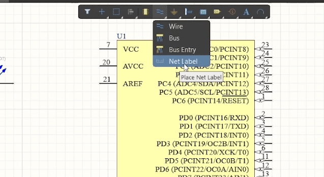
To connect components using netlabels right click on the button here and select netlabel. Now, click on the terminal and this will create a netlabel.
Let’s say I want to connect pin number 19 to the resistor. Let’s give this Netlabel a name – LEDPin

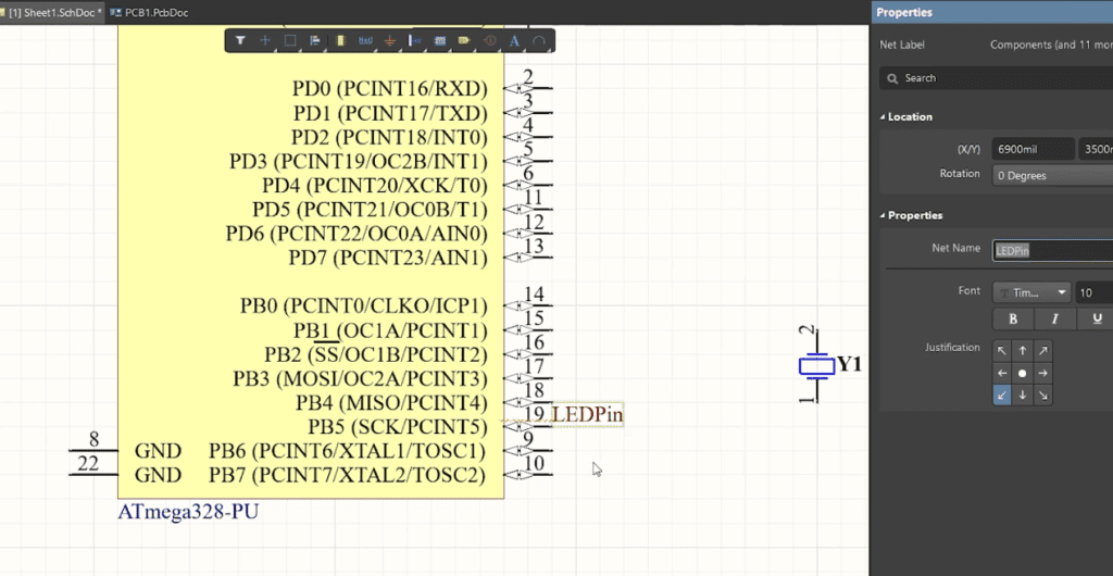
Now to connect this point to another terminal, say at one terminal of the resistor, simply create a Netlabel there, and select the netlabel as LEDPin. Both these terminals have LEDPin netlabels which means, they are physically connected.

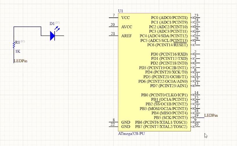
Using netlabels will help us to arrange all the components properly and the circuit looks neat and tidy, especially in the case of large circuits. So let’s connect the remaining components.

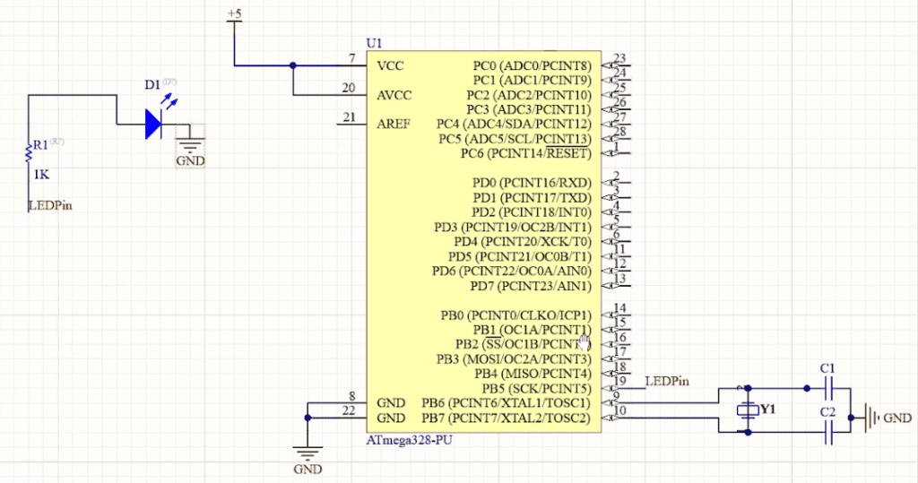
Alright. The bare minimum circuit is now ready. Once you power up the atmega328, it will work. But that is not enough, is it? We will, be making it more stable, versatile, and more USEFUL. Let’s make it closer to the real Arduino Board.

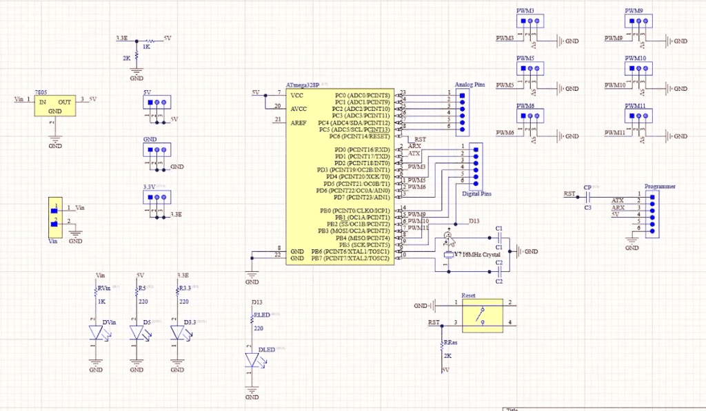
Here I have added a few more components and some headers so that the Arduino looks more like the original Arduino and also, we can use all of the GPIO pins for our project.
So the circuit is complete and now let’s design the PCB.
Altium 365
There is another awesome feature I would like to show you. There is something called Altium 365 that comes free with Altium Subscription.

With Altium 365, you can design, share, manufacture, and do everything related to your project in the same space without any extra effort. You can also share your designs, and ideas and easily collaborate with your teammates or even clients with Secure Centralized Cloud Storage.
Altium Tutorial Step 3 – Designing the PCB
Adding the Components and Nets to the PCB File
Now, to design the PCB, first, you need to save the schematic file.

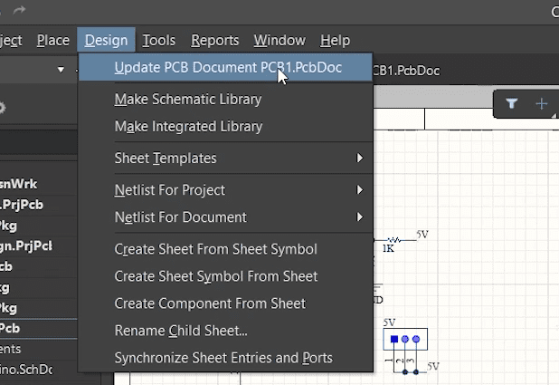
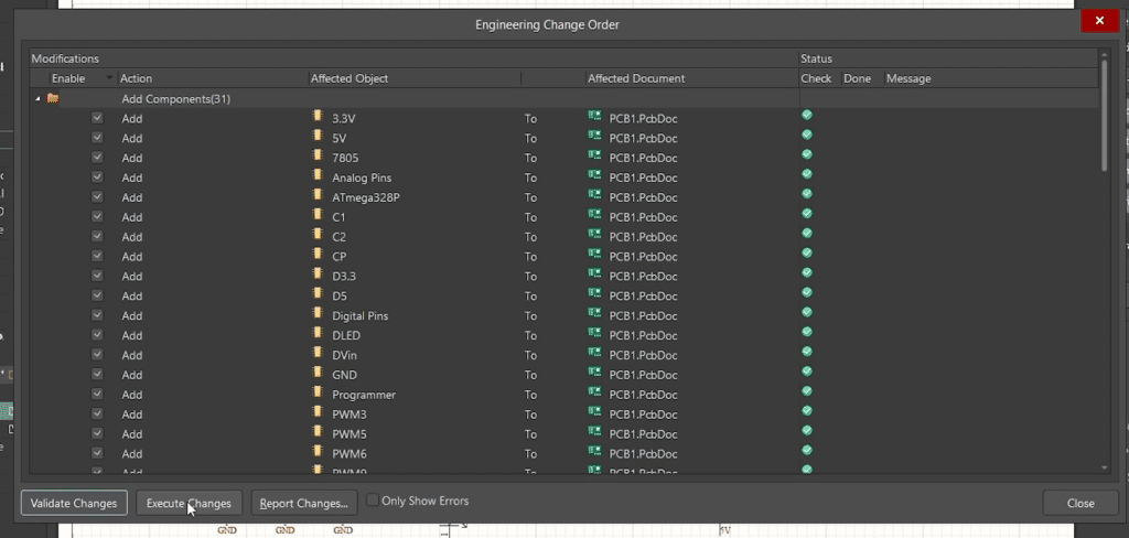
While in the schematics file goes to design and click on update PCB document and this window will appear. Make sure all the components and nets are selected now click on validate changes. And then click on execute changes.

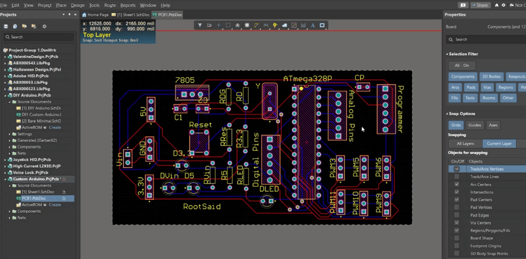
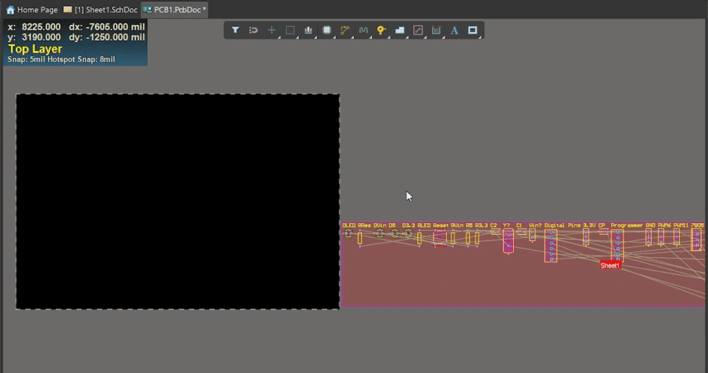
Now you are in the PCB file and here you can see all the components and nets are added to the PCB file.

Designing the Board Shape
Here you can see a black portion and a gray portion, right? The black portion is actually the PCB. But we don’t need this much area for our simple Arduino circuit, so let’s redesign the board to fit our components properly.
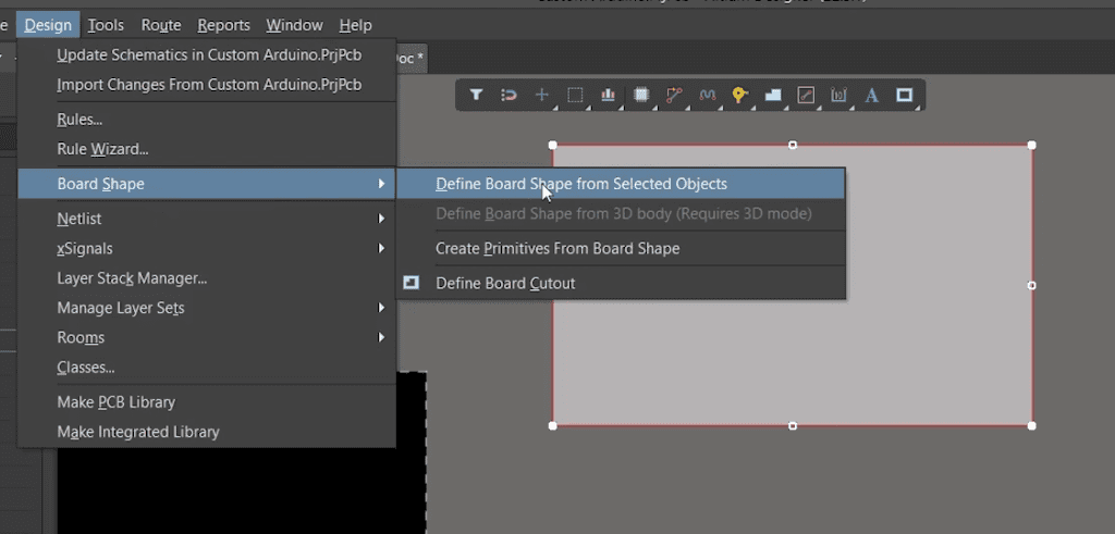
Go to drawing tools, right-click on that, and select Rectangle. Draw a rectangle around your components — make sure all the components and routes will comfortably fit inside it.
Now select that rectangle, and follow this exact menu path:
Design » Board Shape » Define Board Shape from Selected Objects
That’s it — the board shape will now change to match the rectangle you drew. All you have to do next is place all the components inside this new board area and arrange them however you want.
How to Edit and Modify Board Shape in Altium Designer
This is one of the most searched questions from beginners, so let me break it down clearly. Altium has a dedicated Board Planning Mode and several board shape commands — here’s exactly how each one works:
Step 1 — Enter Board Planning Mode
Press the number key 1 on your keyboard (not the numpad). This switches you into Board Planning Mode. You can also get there via View » Board Planning Mode.
Step 2 — Edit Board Shape (vertex editing)
To edit the board outline by moving individual corner points (vertices), use:
Design » Edit Board Shape
This lets you click and drag individual vertices to reshape the board outline precisely.
Step 3 — Modify Board Shape (resizing)
To resize the overall board by dragging the edges, use:
Design » Modify Board Shape
Click and drag the dots around the board edge to expand or shrink the board area.
Step 4 — Return to Normal View
When you’re done editing, press the number key 2 to return to the standard 2D PCB view.
Pro Tip: Use Design » Edit Board Shape for precise vertex-by-vertex editing and Design » Modify Board Shape when you just need to quickly resize the overall board outline.
Here’s a quick reference for all the board shape commands you’ll use:
| Command | Menu Path | What It Does |
|---|---|---|
| Define Board Shape | Design » Board Shape » Define from Selected Objects | Sets board outline from a drawn shape |
| Edit Board Shape | Design » Edit Board Shape | Move individual vertices of the board outline |
| Modify Board Shape | Design » Modify Board Shape | Drag edges to resize the overall board |
| Redefine Board Shape | Design » Board Shape » Redefine Board Shape | Redraw the board outline from scratch |
| Board Planning Mode | View » Board Planning Mode (or press 1) | Switches to the board editing view |
| Return to 2D View | Press 2 | Returns to normal PCB layout view |

Mind the Layers!
One thing you should keep in mind is every PCB has a top side and a bottom side right and some PCBs have some layer in between. While placing a component you have to make sure the component that you are placing is in the right layer.
Since this is a beginner’s tutorial I will be placing all the components on the top layer. To check on which layer the component is currently in simply click on the component and under properties you should see the layer see the switch is in the top layer, the resistor is in the top layer and LEDs are in the top layer.

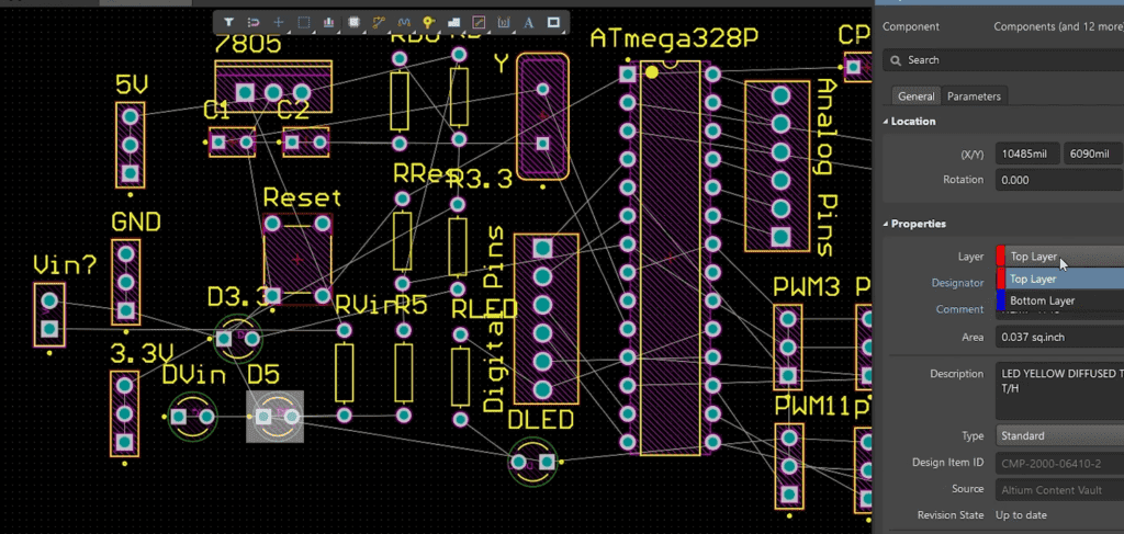
Now if you want to change it from the top layer to the bottom layer simply click on the component and under properties select the bottom layer.
Routing the Components inside PCB
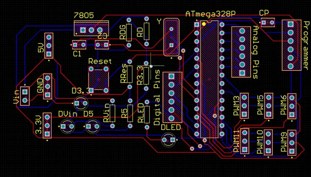
Our work is almost done guys now all you have to do is route all the components. To do that go to this routing tool, right-click on that, and select interactive routing.

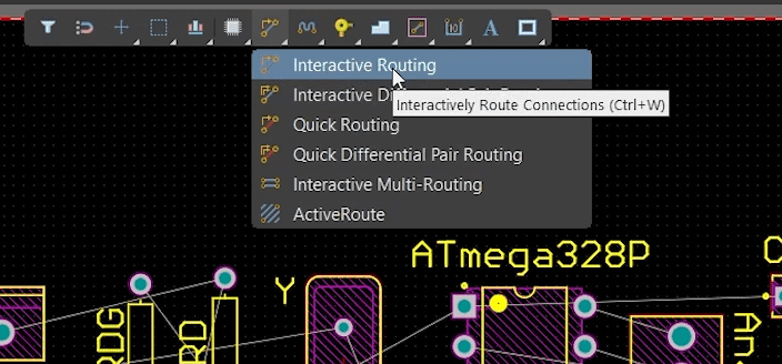
Here you can see the cursor has changed. Now click on the first terminal of the resistor and if you move the mouse, you can see a route is being placed. Now click on the terminal on the LED and that’s it.

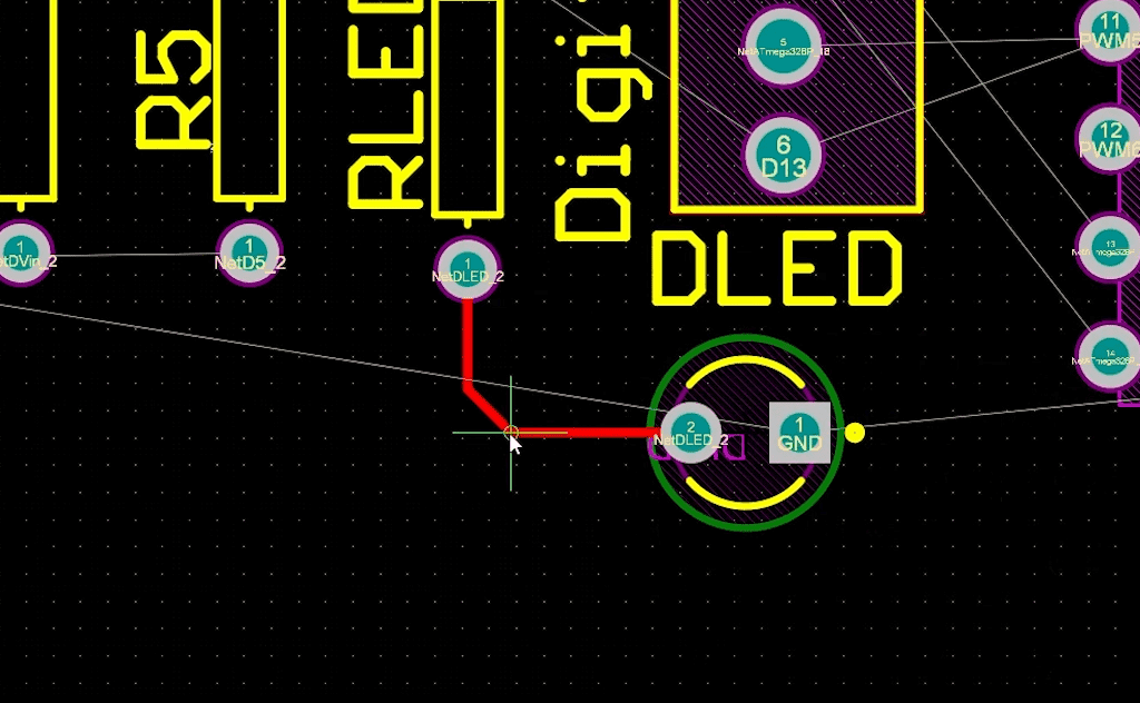
The first route has been added we can easily do the same for all the remaining nets.

Running Design Rule Check (DRC) in Altium
Alright, routing is done — but before we move on, there’s one critical step that most beginner tutorials skip entirely: running the Design Rule Check, or DRC. Trust me, don’t skip this. The DRC is what catches all the little errors in your PCB layout before you send it off for manufacturing. Finding a short circuit or a clearance violation after you’ve already ordered your boards is a painful (and expensive) lesson.
Here’s how to run it:
1. From the top menu, go to Tools » Design Rule Check
2. The DRC dialog box will open. For a beginner project like our Arduino board, the default rules are fine — just click Run Design Rule Check at the bottom.
3. Altium will scan your entire PCB layout and generate a report listing all violations it finds.
Common errors beginners run into:
- Clearance Violation — Two copper tracks or pads are too close together. Fix this by rerouting the offending track with a bit more spacing between it and the neighboring copper.
- Unrouted Net — You forgot to route a connection between two pads. The DRC will highlight exactly which net is missing. Go back to interactive routing and complete it.
- Short Circuit — Two different nets are accidentally touching. This one is critical — a short circuit on a real PCB will either prevent it from working or damage your components.
After the DRC runs, you’ll see a Messages panel at the bottom of the screen listing all the errors. You can click on any error in that list and Altium will zoom directly to the problem area on your PCB. Fix each one, then run the DRC again until you get a clean result — ideally 0 errors, 0 warnings.
Once your DRC comes back clean, your PCB layout is genuinely ready. Now let’s get it manufactured.
Adjusting Board Shape/Size
Guys now our PCB is ready. if we zoom out and take a look at the PCB, we can see that there’s a lot of empty space around the components right? So we can edit the board shape. For that press on number key 1 to enter the board planning mode.

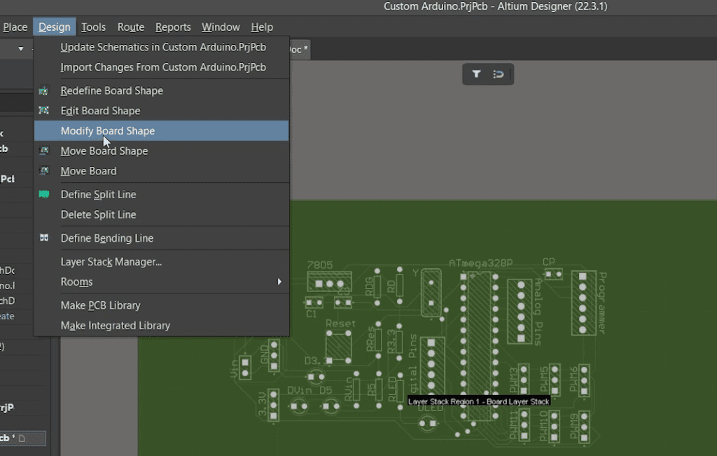
From the top menu, go to Design, Modify Board Shape. Now you can simply edit the board shape, by clicking and dragging the dots around the board.

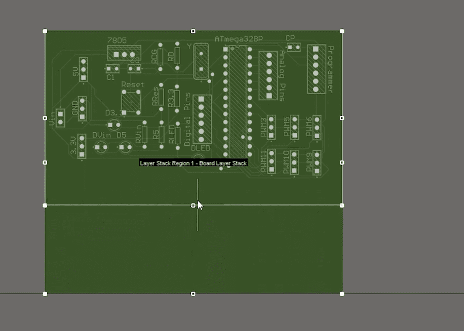
Once done, you can go back to the previous view by pressing number key 2.
Adding Text
All right. Our PCB is now finished now if you want you can add text and images to our PCB.
To add text, click on the string, click on the position where you want to apply the string, and press escape. Now double click on the string and under the text you can change the text. Let’s change it to root set and hit enter.

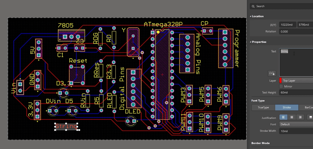
We have placed the text to rotate it simply press on the spacebar all right so basically, this is how you draw a circuit and design a PCB layout for your DIY project using Altium.
Generating Gerber Files for PCB Manufacturing
So your PCB design is complete, the DRC is clean, and you’re ready to actually get this thing made. The way you send your PCB design to a manufacturer is by generating Gerber files — these are the industry-standard files that every PCB fab house understands. Here’s exactly how to generate them in Altium:
Generating Gerber Files
1. From the top menu, go to File » Fabrication Outputs » Gerber Files
2. The Gerber Setup dialog will open. For a standard 2-layer board like our Arduino project, the default settings work perfectly. Make sure the Units are set to Millimeters and Format is 4:4.
3. Click OK — Altium will generate all the Gerber layers and open them in the CAM editor so you can visually verify they look correct.
Generating NC Drill Files
Gerber files alone aren’t enough — you also need NC Drill files so the manufacturer knows where to drill the holes for through-hole components and vias.
1. Go to File » Fabrication Outputs » NC Drill Files
2. Keep the default settings and click OK
3. Altium will generate the .DRL files alongside your Gerbers
Is Altium Designer free to use?
Altium Designer is not free for professionals — it’s a paid commercial software. However, there are two ways to use it at no cost. First, there’s a free trial available on the Altium website. Second, and more useful for most of our readers, Altium offers a free student license through the Altium Education program. This license is renewable every 6 months as long as you’re enrolled in an academic institution. So if you’re a student, you essentially have free access for your entire degree.
What’s the difference between the Schematic file and the PCB file in Altium?
The Schematic file (.SchDoc) is where you draw your circuit — components, connections, net labels, power symbols. Think of it as the logical diagram of your circuit. The PCB file (.PcbDoc) is where the physical layout lives — the actual copper tracks, pad positions, board outline, and layer stack. In Altium, you push your schematic into the PCB file using Design » Update PCB Document, which transfers all your components and their connections into the physical layout environment.
How do I fix a “component has no footprint” error in Altium?
This is one of the most common errors beginners hit. It means the component you placed in the schematic doesn’t have a physical footprint assigned to it — so Altium doesn’t know how to place it on the PCB. To fix it: double-click the component in the schematic, go to the Models section in the component properties, click Add, select Footprint, and then search for the correct footprint from the Altium library. For most standard components like resistors, capacitors, and ICs, Altium’s built-in library will have the right footprint.
Can I use Altium Designer on a Mac?
Altium Designer is a Windows-native application and does not have a native Mac version. If you’re on a Mac, your options are to run it through Boot Camp (installing Windows natively on your Mac), using a virtual machine like Parallels Desktop or VMware Fusion running Windows, or using a Windows cloud PC. Altium 365 does have a web-based viewer that works in any browser, but the full design environment requires Windows.
How long does it take to learn Altium Designer as a beginner?
For basic PCB design like the Arduino board project in this tutorial, most people are comfortable within a few hours of hands-on practice. Following this tutorial end-to-end should take you roughly 30–60 minutes for the first run. Getting proficient with advanced features like multi-layer design, differential pairs, and impedance-controlled routing takes longer — but the fundamentals you learn here apply to everything.